In a just-published paper in the magazine Science, IBM researchers demonstrated a radio-frequency graphene transistor with the highest cut-off frequency achieved so far for any graphene device — 100 billion cycles/second (100 GigaHertz).
This accomplishment is a key milestone for the Carbon Electronics for RF Applications (CERA) program funded by DARPA, in an effort to develop next-generation communication devices.
The high frequency record was achieved using wafer-scale, epitaxially grown graphene using processing technology compatible to that used in advanced silicon device fabrication.
“A key advantage of graphene lies in the very high speeds in which electrons propagate, which is essential for achieving high-speed, high-performance next generation transistors,” said Dr. T.C. Chen, vice president, Science and Technology, IBM Research. “The breakthrough we are announcing demonstrates clearly that graphene can be utilized to produce high performance devices and integrated circuits.”
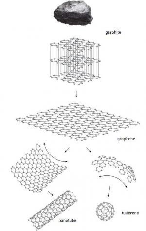
Graphene is a single atom-thick layer of carbon atoms bonded in a hexagonal honeycomb-like arrangement. This two-dimensional form of carbon has unique electrical, optical, mechanical and thermal properties and its technological applications are being explored intensely.
Uniform and high-quality graphene wafers were synthesized by thermal decomposition of a silicon carbide (SiC) substrate. The graphene transistor itself utilized a metal top-gate architecture and a novel gate insulator stack involving a polymer and a high dielectric constant oxide. The gate length was modest, 240 nanometers, leaving plenty of space for further optimization of its performance by scaling down the gate length.
It is noteworthy that the frequency performance of the graphene device already exceeds the cut-off frequency of state-of-the-art silicon transistors of the same gate length (~ 40 GigaHertz). Similar performance was obtained from devices based on graphene obtained from natural graphite, proving that high performance can be obtained from graphene of different origins. Previously, the team had demonstrated graphene transistors with a cut-off frequency of 26 GigaHertz using graphene flakes extracted from natural graphite.
Story Source:
The above story is reprinted from materials provided by IBM.
Dr Ponomarenko, who carried out this work, shows his research sample: graphene quantum dots on a chip. (Credit: Image courtesy of University of Manchester)
Researchers have used the world’s thinnest material to create the world’s smallest transistor, one atom thick and ten atoms wide. Reporting their peer-reviewed findings in the journal Science, Dr Kostya Novoselov and Professor Andre Geim from The School of Physics and Astronomy at The University of Manchester show that graphene can be carved into tiny electronic circuits with individual transistors having a size not much larger than that of a molecule.
The smaller the size of their transistors the better they perform, say the Manchester researchers.
In recent decades, manufacturers have crammed more and more components onto integrated circuits. As a result, the number of transistors and the power of these circuits have roughly doubled every two years. This has become known as Moore’s Law.
But the speed of cramming is now noticeably decreasing, and further miniaturisation of electronics is to experience its most fundamental challenge in the next 10 to 20 years, according to the semiconductor industry roadmap.
At the heart of the problem is the poor stability of materials if shaped in elements smaller than 10 nanometres* in size. At this spatial scale, all semiconductors — including silicon — oxidise, decompose and uncontrollably migrate along surfaces like water droplets on a hot plate.
Four years ago, Geim and his colleagues discovered graphene, the first known one-atom-thick material which can be viewed as a plane of atoms pulled out from graphite. Graphene has rapidly become the hottest topic in physics and materials science.
Now the Manchester team has shown that it is possible to carve out nanometre-scale transistors from a single graphene crystal. Unlike all other known materials, graphene remains highly stable and conductive even when it is cut into devices one nanometre wide.
Graphene transistors start showing advantages and good performance at sizes below 10 nanometres – the miniaturization limit at which the Silicon technology is predicted to fail.
“Previously, researchers tried to use large molecules as individual transistors to create a new kind of electronic circuits. It is like a bit of chemistry added to computer engineering”, says Novoselov. “Now one can think of designer molecules acting as transistors connected into designer computer architecture on the basis of the same material (graphene), and use the same fabrication approach that is currently used by semiconductor industry”.
“It is too early to promise graphene supercomputers,” adds Geim. “In our work, we relied on chance when making such small transistors. Unfortunately, no existing technology allows the cutting materials with true nanometre precision. But this is exactly the same challenge that all post-silicon electronics has to face. At least we now have a material that can meet such a challenge.”
“Graphene is an exciting new material with unusual properties that are promising for nanoelectronics”, comments Bob Westervelt, professor at Harvard University. “The future should be very interesting”.
*One nanometre is one-millionth of a millimetre and a single human hair is around 100,000 nanometres in width.
A paper entitled “Chaotic Dirac Billiard in Graphene Quantum Dots” is published in April 17 issue of Science. It is accompanied by a Perspective article entitled “Graphene Nanoelectronics” by Westervelt.
Story Source:
The above story is reprinted from materials provided by University of Manchester.
— Researchers have used the world’s thinnest material to create the world’s smallest transistor, one atom thick and ten atoms wide. Reporting their peer-reviewed findings in the journal Science, Dr Kostya Novoselov and Professor Andre Geim from The School of Physics and Astronomy at The University of Manchester show that graphene can be carved into tiny electronic circuits with individual transistors having a size not much larger than that of a molecule.
The smaller the size of their transistors the better they perform, say the Manchester researchers.
In recent decades, manufacturers have crammed more and more components onto integrated circuits. As a result, the number of transistors and the power of these circuits have roughly doubled every two years. This has become known as Moore’s Law.
But the speed of cramming is now noticeably decreasing, and further miniaturisation of electronics is to experience its most fundamental challenge in the next 10 to 20 years, according to the semiconductor industry roadmap.
At the heart of the problem is the poor stability of materials if shaped in elements smaller than 10 nanometres* in size. At this spatial scale, all semiconductors — including silicon — oxidise, decompose and uncontrollably migrate along surfaces like water droplets on a hot plate.
Four years ago, Geim and his colleagues discovered graphene, the first known one-atom-thick material which can be viewed as a plane of atoms pulled out from graphite. Graphene has rapidly become the hottest topic in physics and materials science.
Now the Manchester team has shown that it is possible to carve out nanometre-scale transistors from a single graphene crystal. Unlike all other known materials, graphene remains highly stable and conductive even when it is cut into devices one nanometre wide.
Graphene transistors start showing advantages and good performance at sizes below 10 nanometres – the miniaturization limit at which the Silicon technology is predicted to fail.
“Previously, researchers tried to use large molecules as individual transistors to create a new kind of electronic circuits. It is like a bit of chemistry added to computer engineering”, says Novoselov. “Now one can think of designer molecules acting as transistors connected into designer computer architecture on the basis of the same material (graphene), and use the same fabrication approach that is currently used by semiconductor industry”.
“It is too early to promise graphene supercomputers,” adds Geim. “In our work, we relied on chance when making such small transistors. Unfortunately, no existing technology allows the cutting materials with true nanometre precision. But this is exactly the same challenge that all post-silicon electronics has to face. At least we now have a material that can meet such a challenge.”
“Graphene is an exciting new material with unusual properties that are promising for nanoelectronics”, comments Bob Westervelt, professor at Harvard University. “The future should be very interesting”.
*One nanometre is one-millionth of a millimetre and a single human hair is around 100,000 nanometres in width.
A paper entitled “Chaotic Dirac Billiard in Graphene Quantum Dots” is published in April 17 issue of Science. It is accompanied by a Perspective article entitled “Graphene Nanoelectronics” by Westervelt.
Story Source:
The above story is reprinted (with editorial adaptations by ScienceDaily staff) from materials provided by University of Manchester
The Royal Swedish Academy of Sciences has awarded the Nobel Prize in Physics for 2010 to Andre Geim and Konstantin Novoselov, both of the University of Manchester, “for groundbreaking experiments regarding the two-dimensional material graphene.”
Graphene Eloboration
A thin flake of ordinary carbon, just one atom thick, lies behind this year’s Nobel Prize in Physics. Geim and Novoselov have shown that carbon in such a flat form has exceptional properties that originate from the remarkable world of quantum physics.
Graphene is a form of carbon. As a material it is completely new — not only the thinnest ever but also the strongest. As a conductor of electricity it performs as well as copper. As a conductor of heat it outperforms all other known materials. It is almost completely transparent, yet so dense that not even helium, the smallest gas atom, can pass through it. Carbon, the basis of all known life on earth, has surprised us once again.
Geim and Novoselov extracted the graphene from a piece of graphite such as is found in ordinary pencils. Using regular adhesive tape they managed to obtain a flake of carbon with a thickness of just one atom. This at a time when many believed it was impossible for such thin crystalline materials to be stable.
However, with graphene, physicists can now study a new class of two-dimensional materials with unique properties. Graphene makes experiments possible that give new twists to the phenomena in quantum physics. Also a vast variety of practical applications now appear possible including the creation of new materials and the manufacture of innovative electronics. Graphene transistors are predicted to be substantially faster than today’s silicon transistors and result in more efficient computers.
Since it is practically transparent and a good conductor, graphene is suitable for producing transparent touch screens, light panels, and maybe even solar cells.
When mixed into plastics, graphene can turn them into conductors of electricity while making them more heat resistant and mechanically robust. This resilience can be utilised in new super strong materials, which are also thin, elastic and lightweight. In the future, satellites, airplanes, and cars could be manufactured out of the new composite materials.
This year’s Laureates have been working together for a long time now. Konstantin Novoselov, 36, first worked with Andre Geim, 51, as a PhD-student in the Netherlands. He subsequently followed Geim to the United Kingdom. Both of them originally studied and began their careers as physicists in Russia. Now they are both professors at the University of Manchester.
Story Source:
The above story is reprinted from materials provided by Nobel Foundation.
