Technology News

contains news about the latest technologies around the world

Have you ever dreamed of your own air vehicle so you can travel all the way flying anywhere and reach your destinations in shortest time, so here is the vehicle of your dreams, the HOVERBIKE. It is your private helicopter.  Hoverbike is a bike which functions same as the motorbike but the difference is that motor bike travels on roads and the Hoverbike travels in air. Hoverbike is now in manufacturing process and almost completed by the Australians engineers while nowadays they are performing some test on its flight and defining its specification step by step after experiments. They say that these bikes will be available to you soon. Now below we discuss some important parameters and specification of this bike and see how this bike works. I am also embedding some pictures of Hoverbike which is taken from the official site of Hoverbike and are captured by the manufacturers.
[houdini]


The structure of Hoverbike look likes the road bike if it’s both wheel rotated 90°. It has a seat in its middle and to provide the thrust there are two fans on the front and back. In the first design of Hoverbike single blade fan is used however according to the manufacturer, modification is expected in the next models of Hoverbike. Hoverbike functions same as a normal bike it has a throttle through which you can vary its thrust, it has a handle through which you can turn the Hoverbike right and left although it’s turning is not very immediate as the road bike because it will be in air. Hoverbike has a dry weight of 110 kg and it can have maximum weight of 270 kg with fuel and driver. The fuel consumption of the Hoverbike is considerable it burns 0.5litres in 1 minute and for a ride of 1 hour you will need 30 liters of fuel. Hoverbike can have two fuel tanks. The built in tank have 30 liters capacity while an extra fuel can also be added to it and this will increase the fuel capacity of Hoverbike up to 60 liters. The cost of Hoverbike according to the manufacturers of Hoverbike is approximately $45,000AUD +/-$5000. Some other main specifications are given below:

  • Airspeed Vne – 150 KIAS (untested)
  • Hover (out of ground effect) – >10,000ft (estimated)
  • Dry weight – 110kg
  • Max gross weight – 270kg
  • Total thrust – 295kg
  • Engine – 80kw @ 7500rpm


More detailed Specification:

Engine Type:                           flat twin 4-stroke, one camshaft and 4-valves per cylinder, central balancer shaft

Engine Displacement:             1170cc

Bore& Stroke:                         101mm x 73mm

Compression Ratio:                 12.0:1

Nominal Output:                     @7500rpm 80KW

Cooling:                                  Aircooled

Ignition:                                  Electronic

Fuel System:                           Electronic intake pipe injection

Fuel tank capacity(without secondary tanks):                        30L

Fuel tank capacity (with secondary tanks):                60L

Fuel Burn:                               0.5L/min / 30L/hr

Fuel Type:                               Regular Unleaded

Drive-shafts:                           Custom Carbon fiber

Gearbox:                                 Custom 1.5:1 reduction

Propellers:                               2 x Tasmanian Oak with carbon fiber leading edge (made by Michael Ellinas from Heliptera)

Airframe:                                 Carbon fiber with Kevlar reinforcement and foam core

Airframe width:                      1.3m

Airframe length:                      3m

Airframe height:                      0.55m

Dry Weight:                            105kg

Maximum takeoff weight:      270kg

Total Thrust:                            295kg

Range:                                     148km on primary tank @ 80knts cruise (290km with secondary tanks installed)

Airspeed Vne:                         150 KIAS (untested)

Hover:                                                 greater than 10,000ft (estimated)


Hoverbike Applications:

  • Aerial Cattle mustering
  • Search and Rescue
  • Aerial Survey
  • Wildlife and Parks
  • Film
  • Power-line Inspection


Samsung Electro-Mechanics announced Thursday that it has developed a micro-fuel cell and hydrogen generator that runs on H2O.

“When the handset is turned on, metal and water in the phone react to produce hydrogen gas,” explained Oh Yong-soo, vice president of Samsung Electro-Mechanics’ research center. “The gas is then supplied to the fuel cell where it reacts with oxygen in the air to generate power.” Other fuel cells need methanol to produce hydrogen, while Samsung’s needs only water.

Since the micro-fuel cell can generate up to three watts of electricity, it could be used in mobile devices, the company said. The new fuel cell could power a handset for 10 hours, twice as long as rechargeable batteries.

“If the user uses the phone for four hours a day on average, they would have to change the hydrogen cartridge about every five days,” Oh said. “Later handsets will be developed that don’t need the hydrogen cartridges to be changed, and would only need to be filled with water.”

The water-powered cell phones are expected to enter the market by 2010. Samsung Electro-Mechanics unveiled the new technology at the 2007 Korea Electronics Show at the Korea International Exhibition Center in Ilsan, Gyeonggi Province.

So get ready for the water powered mobile phones, there might be a time in the future where you say my phone is running out of water instead of low battery!

For mobile devices, MIPS Technologies offers a range of processor cores and architectures, from small footprint cores with advanced levels of code compression, to some of the industry’s highest performing multiprocessing solutions. MIPS processors offer high performance, low power consumption and cost efficiency supported by a rapidly expanding mobile ecosystem.

Ingenic Semiconductor Licenses MIPS32® Architecture for Mobile Devices

MIPS Technologies Continues Push into Mobile Market

MIPS Technologies, Inc., a leading provider of industry-standard processor architectures and cores for digital consumer, home networking, wireless, communications and business applications, announced today that Ingenic Semiconductor, a leading China-based CPU provider for mobile multimedia applications, has licensed the MIPS32® architecture for its mobile device SoCs. Ingenic is leveraging the MIPS® architecture for devices targeting a broad range of mobile products including e-readers, tablets and smartphones leveraging the Android™ platform.

“The Ingenic team has strong processor design capabilities, and represents a vibrant local semiconductor industry in China. We are pleased to work closely with the company as it brings its innovative XBurst CPU technology to the U.S. market,” said Sandeep Vij, president and CEO, MIPS Technologies. “Innovative companies such as Ingenic are increasingly looking to the MIPS architecture as a high-performance, low-power alternative for mobile designs.”

“Ingenic has had success in the Greater China market with a broad range of small form factor devices, having shipped more than 25 million products to-date,” said Qiang Liu, chairman and CEO for Ingenic Semiconductor. “Our XBurst CPU technology features the high performance, low power and high level of integration needed for success in the mobile market. MIPS Technologies’ industry-standard architecture and broad ecosystem of third party support will be a great help as we continue to expand our business.”

The company will show two MIPS-Based smartphones and several MIPS-Based tablets. Devices are based on systems-on-chips (SoCs) from MIPS licensees including Actions Semiconductor and Ingenic Semiconductor.

The MIPS-Based tablets featuring the Ingenic SoCs are available now. Velocity Micro offers the Cruz Tablets, which can be purchased through major retailers including Amazon, Best Buy, Walmart.com, Borders and many others.

More information on these products is available at www.cruzreader.com. The two smartphones are in pre-production now. Further details will be disclosed in the coming weeks. To schedule a demonstration of MIPS-Based mobile devices, contact [email protected].

“Less than a year ago, MIPS announced its intention to enter the mobile market, leveraging a confluence of industry dynamics and technologies including the Android™ platform and the move to 4G networks. We have signed more than eight mobile-related customers to-date for applications processing, media processing, baseband processing and other technologies in e-readers, tablets, netbooks and mobile handsets. The fact that we can now show these devices—including MIPS-Based smartphones—is a solid endorsement of our strategy,” said  President and CEO, MIPS Technologies.

An Astrolabe is a historical astronomical instrument used by astronomers, navigators, and astrologers. Its many uses include locating and predicting the positions of the Sun, Moon, planets, and stars; determining local time given local latitude and vice-versa; surveying; triangulation; and to cast horoscopes. They were used in Classical Antiquity and through the Islamic Golden Age and the European Middle Ages and Renaissance for all these purposes. In the Islamic world, they were also used to calculate the Qibla and to find the times for Salah, prayers. Here is a video demonstration of an ancient Astrolabe by Tom Wujec.

Bend desk is a future technology which is exactly like a touch screen but have cured surface and multiple new capabilities over simple touch screen. It allows multitasking and multiple user interfacing in the same time. The folks at Media Computing Group have recently re-defined their latest technology BendDesk. This is truly cutting-edge stuff. BendDesk is a multi-touch desk environment that seamlessly combines a vertical and a horizontal touch surface with a curve into one large interactive workspace. Before you start wondering whether this is just another never-to-see-day-of-light concept, we can tell you its not only just an idea anymore.
It is fully functional screen in which you can perform function by physical manipulating the screen. It recognize the multi-touch gestures. the video demo given below gives you more understanding about the interface of this technology. We hope that this technology require few years.

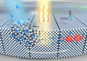
Artist view of the implantation of gallium ions (animated in blue) into germanium wafers followed by a reconstruction of the lattice using short-term flash-lamp annealing and, finally, of the observation of superconductivity at low temperatures. Other than in normal conductors, superconductivity is caused by the formation of electron pairs with anti-parallel momentum and spin (animated in red). (Credit: Sander Münster, Kunstkosmos)

Superconductors are substances that conduct electricity without losses when cooled down to very low temperatures. Pure semiconductors, like silicon or germanium, are almost non-conducting at low temperatures, but transform into conducting materials after doping with foreign atoms. An established method of doping is ion implantation (ions = charged atoms) by which foreign ions are embedded into the crystal lattice of a semiconductor. To produce a superconducting semiconductor, an extreme amount of foreign atoms are necessary, even more than the substance would usually be able to absorb. At the FZD, germanium samples were doped with about six gallium atoms per 100 germanium atoms. With these experiments, the scientists could prove indeed that the doped germanium layer of only sixty nanometers thickness became superconducting, and not just the clusters of foreign atoms which could easily form during extreme doping .

As the germanium lattice is heavily damaged by ion implantation, it has to be repaired afterwards. For such purposes, a flash-lamp annealing facility has been developed at the FZD. Its application allows for a repair of the destroyed crystal lattice by rapidly heating the sample surface (within few milliseconds) while the distribution of the dopant atoms is kept almost the same.

From a scientific point of view, the new material is very promising. It exhibits a surprisingly high critical magnetic field with respect to the temperature where the substance becomes superconducting. For many materials, superconductivity occurs only at very low temperatures, slightly above the absolute zero point of -273 degrees Celsius or 0 Kelvin. The gallium doped germanium samples become superconducting at about 0.5 Kelvin; however, the FZD researchers expect the temperature to increase further by changing various parameters during ion implantation or annealing.

Physicists have been dreaming about superconducting semiconductors for a long time, but saw only few chances for the semiconductor germanium to become superconducting at all. Germanium used to be the material for the first generation of transistors; however, it was soon replaced by silicon, the current material for microelectronics. Recently, the “old” semiconductor material germanium has aroused more and more interest, as it allows, compared to silicon, for more rapid circuits.

Experts even believe germanium to be rediscovered for micro- and nanoelectronics. The reason for such a renaissance lies in the fact that miniaturization in microelectronics industry using silicon is coming to an end. Today, extremely thin oxide layers are needed for transistors, down to a level where silicon oxide does not work well any more. Germanium as a new material for chips would come along with two big advantages: it would enable both faster processes and further miniaturization in micro- and nanoelectronics. Superconducting germanium could thus help to realize circuits for novel computers.

The scientists at the Forschungszentrum Dresden-Rossendorf followed a targeted approach when searching for a new superconducting semiconductor. Instead of doping with boron, which had resulted in superconducting silicon two years ago in France, the scientists choose gallium because of its higher solubility in germanium. In many systematic experiments they proved that the superconductivity of germanium can be reproduced. Furthermore, they were able to show that the transition temperature marking the start of superconductivity can be raised within certain limits.

In the future, the scientists at the two FZD institutes “Ion Beam Physics and Materials Research” and “Dresden High Magnetic Field Laboratory” will combine their know-how in order to fine-tune different rather complex parameters for further experiments, thus hopefully discovering further mysteries of superconducting semiconductors.

Story Source:

The above story is reprinted from materials provided by Forschungszentrum Dresden Rossendorf.

Power Grid of the Future Saves Energy | Power Grid Saves Energy, Cars and trucks race down the highway, turn off into town, wait at traffic lights and move slowly through side streets. Electricity flows in a similar way — from the power plant via high voltage lines to transformer substations. The flow is controlled as if by traffic lights. Cables then take the electricity into the city centre. Numerous switching points reduce the voltage, so that equipment can tap into the electricity at low voltage. Thanks to this highly complex infrastructure, the electricity customer can use all kinds of electrical devices just by switching them on.

“A reliable power supply is the key to all this, and major changes will take place in the coming years to safeguard this reliability. The transport and power networks will grow together more strongly as a result of electromobility, because electric vehicles will not only tank up on electricity but will also make their batteries available to the power grid as storage devices. Renewable energy sources will become available on a wider scale, with individual households also contributing electricity they have generated,” says Professor Lothar Frey, Director of the Fraunhofer Institute for Integrated Systems and Device Technology IISB in Erlangen.

In major projects such as Desertec, solar thermal power plants in sun-rich regions of North Africa and the Middle East will in the future produce electricity for Europe. The energy will then flow to the consumer via long high-voltage power lines or undersea cables. The existing cables, systems and components need to be adapted to the future energy mix now, so that the electricity will get to the consumer as reliably and with as few losses as possible. The power electronics experts at the IISB are working on technological solutions, and are developing components for the efficient conversion of electrical energy.

For energy transmission over distances of more than 500 kilometers or for undersea cables direct current is being increasingly used. This possesses a constant voltage and only loses up to seven percent of its energy over long distances. By comparison, the loss rate for alternating current can reach 40 percent. Additional converter stations are, however, required to convert the high voltage of the direct current into the alternating current needed by the consumer.

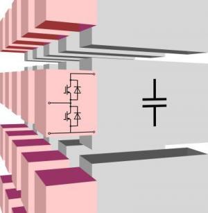
“In cooperation with Siemens Energy we are developing high-power switches. These are necessary for transmitting the direct voltage in the power grid and are crucial for projects like Desertec. The switches have to be more reliable, more scaleable and more versatile than previous solutions in order to meet the requirements of future energy supply networks,” says Dipl.-Ing. Markus Billmann from the IISB. To this end, the research scientists are using low-cost semiconductor cells which with previous switching techniques could not be used for high-voltage direct-current transmission (HVDCT).

“At each end of a HVDCT system there is a converter station,” explains the research scientist. “For the converters we use interruptible devices which can be operated at higher switching frequencies, resulting in smaller systems that are easier to control.” A major challenge is to protect the cells from damage. Each converter station will contain about 5,000 modules, connected in series, and if more than a few of them failed at the same time and affected their neighboring modules a chain reaction could be triggered which would destroy the entire station. “We have now solved this problem. With our cooperation partners we are working on tailor-made materials and components so that in future the equipment will need less energy,” says Billmann.

Story Source:

The above story is reprinted  from materials provided by Fraunhofer-Gesellschaft.

Tags : Power Grid of the Future Saves Energy , Power Grid , Power Grid of the Future , Power Grid of the Future Saves Energy

Now you can imagine the space traveling experience on the earth, the future of transportation is ET3(Evacuated Tube Transport Technologies). This mode of transportation is clean, green, fast, comfortable, safe, faster and affordable.
The traveling time for New york to Beijing is 13 hours 30 minutes through flight while through this technology this time will reduces to 2 hours

The working of ET3 is explained below:
Car sized passenger capsules travel in 1.5m (5′) diameter tubes on frictionless maglev. Air is permanently removed from the two-way tubes that are built along a travel route. Airlocks at stations allow transfer of capsules without admitting air. Linear electric motors accelerate the capsules, which then coast through the vacuum for the remainder of the trip using no additional power. Most of the energy is regenerated as the capsules slow down. ET3 can provide 50 times more transportation per kWh than electric cars or trains.

Speed in initial ET3 systems is 600km/h (370 mph) for in state trips, and will be developed to 6,500 km/h (4,000 mph) for international travel that will allow passenger or cargo travel from New York to Beijing in 2 hours. ET3 is networked like freeways, except the capsules are automatically routed from origin to destination.

This is what the future of transportation.

For more explanation about the ET3 technology watch the video below: