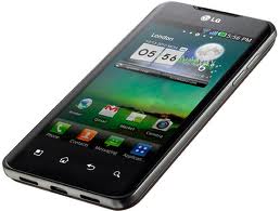
with Tegra 2 introduce the world’s fastest dual-core smartphone with amazing video features and multitasking capabilities. It contains dual-core Tegra2 1GHz processor,it is fully capable of recording videos in crisp 1080p with its 8-megapixel rear camera unit. There’s also a front-facing one at 1.3 megapixels for the video-calling.
Dual-core technology is the next leap forward in mobile technology so this is no small achievement to be the first to offer a smartphone utilizing this technology,” said Dr. Jong-seok Park, CEO and President of LG Electronics Mobile Communications Company. “With unique features such as HDMI (High Definition Multimedia Interface) mirroring and exceptional graphics performance, the LG Optimus 2X is proof of LG’s commitment to high-end smartphones in 2011.”
Developed by graphics processor powerhouse NVIDIA?, the dual-core Tegra 2 system-on-a-chip found in the LG Optimus 2X runs at a clock speed of 1GHz and boasts low power consumption and high performance for playing video and audio. Users will experience faster web browsing and smoother gameplay compared with single-core processors running at the same speed as well as instantaneous touch response and seamless multitasking between applications.
The LG Optimus 2X offers 1080p HD video playback and recording with HDMI mirroring that expands content on external displays to full HD quality. The LG Optimus 2X can connect wirelessly to any DLNA (Digital Living Network Alliance) compatible digital device such as HD TVs for a console-like gaming experience taking full advantage of the phone’s HDMI mirroring, accelerometer and gyro sensor. The smartphone also includes both rear- and front-facing cameras, microSD memory expandability, Micro-USB port and a hefty 1500mAh battery.
The LG Optimus 2X will be available in Korea next month with countries in Europe and Asia to follow. The phone will initially be released with Android 2.2 (Froyo) and will be upgradeable to Android 2.3 (Gingerbread). The upgrade schedule will be announced in local markets in due course.
Key specifications:
– 1Ghz Dual-core Processor (NVIDIA Tegra 2)
– 4-inch WVGA screen
– 8GB memory (up to 32GB via microSD)
– 1,500 mAh battery
– 8 megapixel rear camera and 1.3 megapixel front camera
– HDMI mirroring
– 1080p MPEG-4/H.264 playback and recording
Wind turbines. (Credit: Image courtesy of Delft University of Technology)
Research by TU Delft shows that Dutch power stations are able to cope at any time in the future with variations in demand for electricity and supply of wind power, as long as use is made of up-to-date wind forecasts. PhD candidate Bart Ummels also demonstrates that there is no need for energy storage facilities. Ummels will receive his PhD on this topic on Thursday 26 February.
Wind is variable and can only partially be predicted. The large-scale use of wind power in the electricity system is therefore tricky. PhD candidate Bart Ummels MSc. investigated the consequences of using a substantial amount of wind power within the Dutch electricity system. He used simulation models, such as those developed by transmission system operator TenneT, to pinpoint potential problems (and solutions).
His results indicate that wind power requires greater flexibility from existing power stations. Sometimes larger reserves are needed, but more frequently power stations will have to decrease production in order to make room for wind-generated power. It is therefore essential to continually recalculate the commitment of power stations using the latest wind forecasts. This reduces potential forecast errors and enables wind power to be integrated more efficiently.
Ummels looked at wind power up to 12 GW, 8 GW of which at sea, which is enough to meet about one third of the Netherlands’ demand for electricity. Dutch power stations are able to cope at any time in the future with variations in demand for electricity and supply of wind power, as long as use is made of up-to-date, improved wind forecasts. It is TenneT’s task to integrate large-scale wind power into the electricity grid. Lex Hartman, TenneT’s Director of Corporate Development: “in a joint effort, TU Delft and TenneT further developed the simulation model that can be used to study the integration of large-scale wind power. The results show that in the Netherlands we can integrate between 4 GW and 10 GW into the grid without needing any additional measures.
Surpluses
Ummels: ‘Instead of the common question ‘What do we do when the wind isn’t blowing?’, the more relevant question is ‘Where do we put all the electricity if it is very windy at night?’. This is because, for instance, a coal-fired power station cannot simply be turned off. One solution is provided by the international trade in electricity, because other countries often can use the surplus. Moreover, a broadening of the ‘opening hours’ of the international electricity market benefits wind power. At the moment, utilities determine one day ahead how much electricity they intend to purchase or sell abroad. Wind power can be better used if the time difference between the trade and the wind forecast is smaller.’
No energy storage
Ummels’ research also demonstrates that energy storage is not required. The results indicate that the international electricity market is a promising and cheaper solution for the use of wind power.
Making power stations more flexible is also better than storage. The use of heating boilers, for instance, means that combined heat and power plants operate more flexibly, which can consequently free up capacity for wind power at night.
The use of wind power in the Dutch electricity system could lead to a reduction in production costs of EUR1.5 billion annually and a reduction in CO2 emissions of 19 million tons a year.
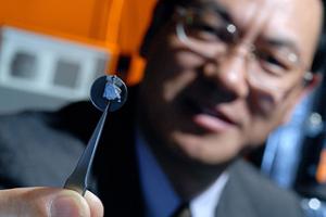
Georgia Tech Professor Zhong Lin Wang holds a sample nanowire array that can be used to power nanometer scale devices. (Georgia Tech Photo: Gary Meek)
Researchers have developed a new technique for powering nanometer-scale devices without the need for bulky energy sources such as batteries.
By converting mechanical energy from body movement, muscle stretching or water flow into electricity, these “nanogenerators” could make possible a new class of self-powered implantable medical devices, sensors and portable electronics.
Described in the April 14th issue of the journal Science, the nanogenerators produce current by bending and then releasing zinc oxide nanowires — which are both piezoelectric and semiconducting. The research was sponsored by the National Science Foundation (NSF), the NASA Vehicle Systems Program and the Defense Advanced Research Projects Agency (DARPA).
“There is a lot of mechanical energy available in our environment,” said Zhong Lin Wang, a Regents Professor in the School of Materials Science and Engineering at the Georgia Institute of Technology. “Our nanogenerators can convert this mechanical energy to electrical energy. This could potentially open up a lot of possibilities for the future of nanotechnology.”
Nanotechnology researchers have proposed and developed a broad range of nanoscale devices, but their use has been limited by the sources of energy available to power them. Conventional batteries make the nanoscale systems too large, and the toxic contents of batteries limit their use in the body. Other potential power sources also suffer from significant drawbacks.
“We can build nanodevices that are very small, but if the complete integrated system must include a large power source, that defeats the purpose,” added Wang, who also holds affiliated faculty positions at Peking University and the National Center for Nanoscience and Technology of China.
The nanogenerators developed by Wang and graduate student Jinhui Song use the very small piezoelectric discharges created when zinc oxide nanowires are bent and then released. By building interconnected arrays containing millions of such wires, Wang believes he can produce enough current to power nanoscale devices.
To study the effect, the researchers grew arrays of zinc oxide nanowires, then used an atomic-force microscope tip to deflect individual wires. As a wire was contacted and deflected by the tip, stretching on one side of the structure and compression on the other side created a charge separation — positive on the stretched side and negative on the compressed side — due to the piezoelectric effect.
The charges were preserved in the nanowire because a Schottky barrier was formed between the AFM tip and the nanowire. The coupling between semiconducting and piezoelectric properties resulted in the charging and discharging process when the tip scanned across the nanowire, Wang explained.
When the tip lost contact with the wire, the strain was released — and the researchers measured an electrical current. After the strain release, the nanowire vibrated through many cycles, but the electrical discharge was measured only at the instant when the strain was released.
To rule out other potential sources of the current, the researchers conducted similar tests using structures that were not piezoelectric or semiconducting. “After a variety of tests, we are confident that what we are seeing is a piezoelectric-induced discharge process,” Wang said.
The researchers grew the nanowire arrays using a standard vapor-liquid-solid process in a small tube furnace. First, gold nanoparticles were deposited onto a sapphire substrate placed in one end of the furnace. An argon carrier gas was then flowed into the furnace as zinc oxide powder was heated. The nanowires grew beneath the gold nanoparticles, which serve as catalysts.
The resulting arrays contained vertically-aligned nanowires that ranged from 200 to 500 nanometers in length and 20 to 40 nanometers in diameter. The wires grew approximately 100 nanometers apart, as determined by the placement of the gold nanoparticles.
A film of zinc oxide also grew between the wires on the substrate surface, creating an electrical connection between the wires. To that conductive substrate, the researchers attached an electrode for measuring current flow.
Though attractive for use inside the body because zinc oxide is non-toxic, the nanogenerators could also be used wherever mechanical energy — hydraulic motion of seawater, wind or the motion of a foot inside a shoe — is available. The nanowires can be grown not only on crystal substrates, but also on polymer-based films. Use of flexible polymer substrates could one day allow portable devices to be powered by the movement of their users.
“You could envision having these nanogenerators in your shoes to produce electricity as you walk,” Wang said. “This could be beneficial to soldiers in the field, who now depend on batteries to power their electrical equipment. As long as the soldiers were moving, they could generate electricity.”
Current could also be produced by placing the nanowire arrays into fields of acoustic or ultrasonic energy. Though they are ceramic materials, the nanowires can bend as much as 50 degrees without breaking.
The next step in the research will be to maximize the power produced by an array of the new nanogenerators. Wang estimates that they can convert as much as 30 percent of the input mechanical energy into electrical energy for a single cycle of vibration. That could allow a nanowire array just 10 microns square to power a single nanoscale device — if all the power generated by the nanowire array can be successfully collected.
“Our bodies are good at converting chemical energy from glucose into the mechanical energy of our muscles,” Wang noted. “These nanogenerators can take that mechanical energy and convert it to electrical energy for powering devices inside the body. This could open up tremendous possibilities for self-powered implantable medical devices.”
Story Source:
The above story is reprinted from materials provided by Georgia Institute of Technology.
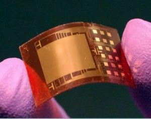
In a new technique for producing nanogenerators, researchers transfer vertically-aligned nanowires to a flexible substrate. (Credit: Courtesy of Zhong Lin Wang)
Blinking numbers on a liquid-crystal display (LCD) often indicate that a device’s clock needs resetting. But in the laboratory of Zhong Lin Wang at Georgia Tech, the blinking number on a small LCD signals the success of a five-year effort to power conventional electronic devices with nanoscale generators that harvest mechanical energy from the environment using an array of tiny nanowires.
In this case, the mechanical energy comes from compressing a nanogenerator between two fingers, but it could also come from a heartbeat, the pounding of a hiker’s shoe on a trail, the rustling of a shirt, or the vibration of a heavy machine. While these nanogenerators will never produce large amounts of electricity for conventional purposes, they could be used to power nanoscale and microscale devices — and even to recharge pacemakers or iPods.
Wang’s nanogenerators rely on the piezoelectric effect seen in crystalline materials such as zinc oxide, in which an electric charge potential is created when structures made from the material are flexed or compressed. By capturing and combining the charges from millions of these nanoscale zinc oxide wires, Wang and his research team can produce as much as three volts — and up to 300 nanoamps.
“By simplifying our design, making it more robust and integrating the contributions from many more nanowires, we have successfully boosted the output of our nanogenerator enough to drive devices such as commercial liquid-crystal displays, light-emitting diodes and laser diodes,” said Wang, a Regents’ professor in Georgia Tech’s School of Materials Science and Engineering. “If we can sustain this rate of improvement, we will reach some true applications in healthcare devices, personal electronics, or environmental monitoring.”
Recent improvements in the nanogenerators, including a simpler fabrication technique, were reported online last week in the journal Nano Letters. Earlier papers in the same journal and in Nature Communications reported other advances for the work, which has been supported by the Defense Advanced Research Projects Agency (DARPA), the U.S. Department of Energy, the U.S. Air Force, and the National Science Foundation.
“We are interested in very small devices that can be used in applications such as health care, environmental monitoring and personal electronics,” said Wang. “How to power these devices is a critical issue.”
The earliest zinc oxide nanogenerators used arrays of nanowires grown on a rigid substrate and topped with a metal electrode. Later versions embedded both ends of the nanowires in polymer and produced power by simple flexing. Regardless of the configuration, the devices required careful growth of the nanowire arrays and painstaking assembly.
In the latest paper, Wang and his group members Youfan Hu, Yan Zhang, Chen Xu, Guang Zhu and Zetang Li reported on much simpler fabrication techniques. First, they grew arrays of a new type of nanowire that has a conical shape. These wires were cut from their growth substrate and placed into an alcohol solution.
The solution containing the nanowires was then dripped onto a thin metal electrode and a sheet of flexible polymer film. After the alcohol was allowed to dry, another layer was created. Multiple nanowire/polymer layers were built up into a kind of composite, using a process that Wang believes could be scaled up to industrial production.
When flexed, these nanowire sandwiches — which are about two centimeters by 1.5 centimeters — generated enough power to drive a commercial display borrowed from a pocket calculator.
Wang says the nanogenerators are now close to producing enough current for a self-powered system that might monitor the environment for a toxic gas, for instance, then broadcast a warning. The system would include capacitors able to store up the small charges until enough power was available to send out a burst of data.
While even the current nanogenerator output remains below the level required for such devices as iPods or cardiac pacemakers, Wang believes those levels will be reached within three to five years. The current nanogenerator, he notes, is nearly 100 times more powerful than what his group had developed just a year ago.
Writing in a separate paper published in October in the journal Nature Communications, group members Sheng Xu, Benjamin J. Hansen and Wang reported on a new technique for fabricating piezoelectric nanowires from lead zirconate titanate — also known as PZT. The material is already used industrially, but is difficult to grow because it requires temperatures of 650 degrees Celsius.
In the paper, Wang’s team reported the first chemical epitaxial growth of vertically-aligned single-crystal nanowire arrays of PZT on a variety of conductive and non-conductive substrates. They used a process known as hydrothermal decomposition, which took place at just 230 degrees Celsius.
With a rectifying circuit to convert alternating current to direct current, the researchers used the PZT nanogenerators to power a commercial laser diode, demonstrating an alternative materials system for Wang’s nanogenerator family. “This allows us the flexibility of choosing the best material and process for the given need, although the performance of PZT is not as good as zinc oxide for power generation,” he explained.
And in another paper published in Nano Letters, Wang and group members Guang Zhu, Rusen Yang and Sihong Wang reported on yet another advance boosting nanogenerator output. Their approach, called “scalable sweeping printing,” includes a two-step process of (1) transferring vertically-aligned zinc oxide nanowires to a polymer receiving substrate to form horizontal arrays and (2) applying parallel strip electrodes to connect all of the nanowires together.
Using a single layer of this structure, the researchers produced an open-circuit voltage of 2.03 volts and a peak output power density of approximately 11 milliwatts per cubic centimeter.
“From when we got started in 2005 until today, we have dramatically improved the output of our nanogenerators,” Wang noted. “We are within the range of what’s needed. If we can drive these small components, I believe we will be able to power small systems in the near future. In the next five years, I hope to see this move into application.”
Scientists say on way to solving anti-matter mystery
Scientists say on way to solving anti-matter mystery, European scientists reported about the creation and capture of anti-hydrogen atoms in a novel magnetic trap and said it put them on track to solving one of the great cosmic mysteries – the make-up of anti-matter.
Anti-matter is of intense interest outside the global scientific community because it has often been cited as a potential source of boundless and almost cost-free energy.
The announcement from CERN, the European Organization for Nuclear Research, came just three weeks after another of the three teams working separately on the problem at the particle research centre near Geneva said they had briefly made and caught the elusive atoms for the first time.
“With these alternative methods of producing and eventually studying anti-hydrogen, anti-matter will not be able to hide its properties from us for much longer,” said Yasunori Yamazaki of the team that scored the latest breakthrough.
Anti, or neutral, matter is believed to have been created in the same quantities as conventional matter – the substance of everything visible in the universe including life on earth – at the moment of the Big Bang 13.7 billion years ago.
A theme of much science fiction, it was only discovered by US physicist David Anderson in 1932.
As the latest breakthrough was reported, CERN engineers were closing down the centre’s showpiece Large Hadron Collider or LHC for a two-month break after eight months of scientific success in research into how the universe began.
Operations extended
CERN’s Director-General Rolf Heuer told Reuters that new discoveries were rolling in so fast that it was likely the initial phase of LHC operations would be stretched to the end of 2012, a year longer than planned.
His deputy Sergio Bertolucci said the LHC was moving rapidly into totally new territories of scientific knowledge and the coming months could bring real insight into the “dark matter” that makes up 25 percent of the universe.
Physicists and cosmologists speculate that “dark matter” – so called because it reflects no light and cannot be seen – could account for at least some of the missing anti-matter, particles which were first spotted at CERN in 2002.
Some suggest it may have also some relation to the “dark energy” that constitutes about 70 percent of the universe leaving only 5 percent for the visible parts – galaxies, stars and planets – that can be observed from earth or nearby.
Monday’s announcement said the “ASACUSA” experiment, in a CERN storage ring known as the Antiproton Decelerator or AD, captured “significant numbers” of anti-hydrogen atoms in flight in a particle trap called CUSP.
Last month the parallel, and complementary, ALPHA experiment at the AD captured 38 anti-hydrogen atoms in flight and held them fleetingly, making possible initial observations of their properties and behaviour.
New equipment developed by ASACUSA, ALPHA and a third experiment, ATRAP, has overcome the problem that prevented close study of anti-particles until now – the fact that when they meet other matter they self-destruct. – Reuters
Tags : Scientists , Scientists says, Scientists say on way to solving , Scientists say on way to solving anti-matter , Scientists say on way to solving anti-matter mystery
This is an artist's illustration of an artificial e-skin with nanowire active matrix circuitry covering a hand. A fragile egg is held, illustrating the functionality of the e-skin device for prosthetic and robotic applications. (Credit: Ali Javey and Kuniharu Takei)
Engineers Make Artificial Skin out of Nanowires
Engineers at the University of California, Berkeley, have developed a pressure-sensitive electronic material from semiconductor nanowires that could one day give new meaning to the term “thin-skinned.”
“The idea is to have a material that functions like the human skin, which means incorporating the ability to feel and touch objects,” said Ali Javey, associate professor of electrical engineering and computer sciences and head of the UC Berkeley research team developing the artificial skin.
The artificial skin, dubbed “e-skin” by the UC Berkeley researchers, is described in a Sept. 12 paper in the advanced online publication of the journal Nature Materials. It is the first such material made out of inorganic single crystalline semiconductors.
A touch-sensitive artificial skin would help overcome a key challenge in robotics: adapting the amount of force needed to hold and manipulate a wide range of objects.
“Humans generally know how to hold a fragile egg without breaking it,” said Javey, who is also a member of the Berkeley Sensor and Actuator Center and a faculty scientist at the Lawrence Berkeley National Laboratory Materials Sciences Division. “If we ever wanted a robot that could unload the dishes, for instance, we’d want to make sure it doesn’t break the wine glasses in the process. But we’d also want the robot to be able to grip a stock pot without dropping it.”
A longer term goal would be to use the e-skin to restore the sense of touch to patients with prosthetic limbs, which would require significant advances in the integration of electronic sensors with the human nervous system.
Previous attempts to develop an artificial skin relied upon organic materials because they are flexible and easier to process.
“The problem is that organic materials are poor semiconductors, which means electronic devices made out of them would often require high voltages to operate the circuitry,” said Javey. “Inorganic materials, such as crystalline silicon, on the other hand, have excellent electrical properties and can operate on low power. They are also more chemically stable. But historically, they have been inflexible and easy to crack. In this regard, works by various groups, including ours, have recently shown that miniaturized strips or wires of inorganics can be made highly flexible — ideal for high performance, mechanically bendable electronics and sensors.”
The UC Berkeley engineers utilized an innovative fabrication technique that works somewhat like a lint roller in reverse. Instead of picking up fibers, nanowire “hairs” are deposited.
The researchers started by growing the germanium/silicon nanowires on a cylindrical drum, which was then rolled onto a sticky substrate. The substrate used was a polyimide film, but the researchers said the technique can work with a variety of materials, including other plastics, paper or glass. As the drum rolled, the nanowires were deposited, or “printed,” onto the substrate in an orderly fashion, forming the basis from which thin, flexible sheets of electronic materials could be built.
In another complementary approach utilized by the researchers, the nanowires were first grown on a flat source substrate, and then transferred to the polyimide film by a direction-rubbing process.
For the e-skin, the engineers printed the nanowires onto an 18-by-19 pixel square matrix measuring 7 centimeters on each side. Each pixel contained a transistor made up of hundreds of semiconductor nanowires. Nanowire transistors were then integrated with a pressure sensitive rubber on top to provide the sensing functionality. The matrix required less than 5 volts of power to operate and maintained its robustness after being subjected to more than 2,000 bending cycles.
The researchers demonstrated the ability of the e-skin to detect pressure from 0 to 15 kilopascals, a range comparable to the force used for such daily activities as typing on a keyboard or holding an object. In a nod to their home institution, the researchers successfully mapped out the letter C in Cal.
“This is the first truly macroscale integration of ordered nanowire materials for a functional system — in this case, an electronic skin,” said study lead author Kuniharu Takei, post-doctoral fellow in electrical engineering and computer sciences. “It’s a technique that can be potentially scaled up. The limit now to the size of the e-skin we developed is the size of the processing tools we are using.”
Other UC Berkeley co-authors of the paper are Ron Fearing, professor of electrical engineering and computer sciences; Toshitake Takahashi, graduate student in electrical engineering and computer sciences; Johnny C. Ho, graduate student in materials science and engineering; Hyunhyub Ko and Paul Leu, post-doctoral researchers in electrical engineering and computer sciences; and Andrew G. Gillies, graduate student in mechanical engineering.
The National Science Foundation and the Defense Advanced Research Projects Agency helped support this research.
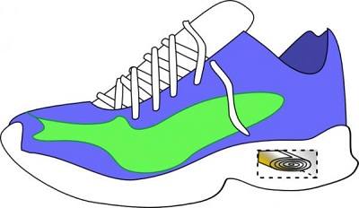
Illustration of Dr. Ville Kaajakari's shoe power generator. (Credit: Image courtesy of Louisiana Tech University)
Dr. Ville Kaajakari, assistant professor of electrical engineering at Louisiana Tech University has developed a technology that harvests power from a small generator embedded in the sole of a shoe.
Kaajakari’s innovative technology, developed at Louisiana Tech’s Institute for Micromanufacturing (IfM), is based on new voltage regulation circuits that efficiently convert a piezoelectric charge into usable voltage for charging batteries or for directly powering electronics.
“This technology could benefit, for example, hikers that need emergency location devices or beacons,” said Kaajakari. “For more general use, you can use it to power portable devices without wasteful batteries.”
The technology is being featured by MEMS Investor Journal, a national online industry publication. MEMS are tiny “smart” devices that combine computer chips with micro-components such as sensors, gears, flow-channels, mirrors and actuators.MEMS Investor Journal is an independent publication that provides investment professionals with the latest developments in the micro electro mechanical systems (MEMS) industry.
According to the article, energy harvesting is an attractive way to power MEMS sensors and locator devices such as GPS. However, power harvesting technologies often fall short in terms of output as many of today’s applications require higher power levels.
Kaajakari’s breakthrough uses a low-cost polymer transducer that has metalized surfaces for electrical contact. Unlike conventional ceramic transducers, the polymer-based generator is soft and robust, matching the properties of regular shoe fillings. The transducer can therefore replace the regular heel shock absorber with no loss in user experience.
In addition to running sensors and inertial navigation, Kaajakari’s shoe power generator can also be used to power RF transponders and GPS receivers.
“Ultimately, we want to bring up the power levels up to a point where we could, in addition to sensors, charge or power other portable devices such as cell phones.”
Article: Microstructured piezoelectric shoe power generator outperforms batteries
Story Source:
The above story is reprinted from materials provided by Louisiana Tech University. The original article was written by Dave Guerin.
In a just-published paper in the magazine Science, IBM researchers demonstrated a radio-frequency graphene transistor with the highest cut-off frequency achieved so far for any graphene device — 100 billion cycles/second (100 GigaHertz).
This accomplishment is a key milestone for the Carbon Electronics for RF Applications (CERA) program funded by DARPA, in an effort to develop next-generation communication devices.
The high frequency record was achieved using wafer-scale, epitaxially grown graphene using processing technology compatible to that used in advanced silicon device fabrication.
“A key advantage of graphene lies in the very high speeds in which electrons propagate, which is essential for achieving high-speed, high-performance next generation transistors,” said Dr. T.C. Chen, vice president, Science and Technology, IBM Research. “The breakthrough we are announcing demonstrates clearly that graphene can be utilized to produce high performance devices and integrated circuits.”
Graphene is a single atom-thick layer of carbon atoms bonded in a hexagonal honeycomb-like arrangement. This two-dimensional form of carbon has unique electrical, optical, mechanical and thermal properties and its technological applications are being explored intensely.
Uniform and high-quality graphene wafers were synthesized by thermal decomposition of a silicon carbide (SiC) substrate. The graphene transistor itself utilized a metal top-gate architecture and a novel gate insulator stack involving a polymer and a high dielectric constant oxide. The gate length was modest, 240 nanometers, leaving plenty of space for further optimization of its performance by scaling down the gate length.
It is noteworthy that the frequency performance of the graphene device already exceeds the cut-off frequency of state-of-the-art silicon transistors of the same gate length (~ 40 GigaHertz). Similar performance was obtained from devices based on graphene obtained from natural graphite, proving that high performance can be obtained from graphene of different origins. Previously, the team had demonstrated graphene transistors with a cut-off frequency of 26 GigaHertz using graphene flakes extracted from natural graphite.
Story Source:
The above story is reprinted from materials provided by IBM.

 it is fully capable of recording videos in crisp 1080p with its 8-megapixel rear camera unit. There’s also a front-facing one at 1.3 megapixels for the video-calling.