Electronics Projects

contains discrete electrical projects without microcontrollers

Abstract

One of the first and most widely used application of power electronic devices have been in rectification. Rectification refers to the process of converting an ac voltage or current source to dc voltage and current. Rectifiers specially refer to power electronic converters where the electrical power flows from the ac side to the dc side. In many situations the same converter circuit may carry electrical power from the dc side to the ac side where upon they are referred to as inverters. We will be Designing and Simulating single phase half wave Rectifier; commonly used rectifier circuits supplying different types of loads (resistive, inductive, capacitive, back emf type) will be presented.

Contents

  • Introduction……………………………………………
  • Objectives of the Project…………………………..
  • Point of interests
  • Circuit Description & Operation………………..
  • Mathematical Analysis…………………………….
  • Computer simulation
    • Software Code
    • Sample Run
    • Outputs
      • Circuit
      • Outputs
      • Block Diagram
      • Outputs

1.      MATLAB Simulation

2.      MATLAB Simulink (Time Domain Implementation)

3.      MATLAB Simulink (Frequency Domain Implementation)

4.      Multisim Implementation…………………………


Introduction

Single phase rectifiers are extensively used in a number of power electronic based converters. In most cases they are used to provide an intermediate unregulated dc voltage source which is further processed to obtain a regulated dc or ac output. They have, in general, been proved to be efficient.


Objectives of the Project:

  • Analyze the operation of single phase half wave rectifier supply resistive, inductive loads.
  • Define and calculate the Performance Parameters of the rectifier.
  • Simulate the circuit with computer software package (MATLAB)
  • In addition to MATLAB we also simulated the project in Multisim


Points of interest in the analysis will be.

•   Waveforms and characteristic values (average, RMS etc) of the rectified voltage and current.

•   Influence of the load type on the rectified voltage and current.

•   Reaction of the rectifier circuit upon the ac network, reactive power requirement, power factor, harmonics etc.

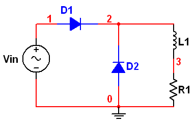
Circuit Description & Operation:

Let the source voltage vs be defined to be E*sin (wt). The source voltage is positive when 0 < wt < pi  radians and it is negative when pi < wt < 2 pi radians. When vs is positive, diode D1 conducts and the voltage vc is positive. This in turn leads to diode D2 being reverse-biased during this period. During  pi < wt < 2 pi the voltage vc would be negative if diode D1 tends to conduct. This means that D2 would be forward-biased and would conduct. When diode D2 conducts, the voltage vc would be zero volts, assuming that the diode drop is negligible. Additionally when diode D2 conducts, diode D1 remains reverse-biased, because the voltage vs is negative. When the current through the inductor tends to fall, it starts acting as a source. When the inductor acts as a source, its voltage tends to forward bias diode D2 if the source voltage vs is negative and forward bias diode D1 if the source voltage vs is positive. Even when the source voltage vs is positive, the inductor current would tend to fall if the source voltage is less than the voltage drop across the load resistor. During the negative half-cycle of source voltage, diode D1 blocks conduction and diode D2 is forced to conduct. Since diode D2 allows the inductor current circulate through L, R and D2, diode D2 is called the free-wheeling diode. We can say that the current free-wheels through D2.

Mathematical Analysis

An expression for the current through the load can be obtained as shown below. It can be assumed that the load current flows all the time. In other words, the load current is continuous. When diode D1 conducts, the driving function for the differential equation is the sinusoidal function defining the source voltage. During the period defined by pi < wt < 2pi, diode D1 blocks current and acts as an open switch. On the other hand, diode D2 conducts during this period, the driving function can be set to be zero volts. For 0 < wt <pi, the equation (1) shown below applies.

For the negative half-cycle of the source, equation (2) applies. As in the previous case, the solution is obtained in two parts. The expressions for the complementary integral and the particular integral are the same. The expression for the complementary integral is presented by equation (3). The particular solution to the equation (1) is the steady-state response and is presented as equation (4). The total solution is the sum of both the complimentary and the particular solution. The total solution is presented as equation (5).

The difference in solution is in how the constant A in complementary integral is evaluated. In the case of the circuit without free-wheeling diode, i(0) = 0, since the current starts building up from zero at the start of every positive half-cycle. On the other hand, the current-flow is continuous when the circuit contains a free-wheeling diode also. Since the input to the RL circuit is a periodic half-sinusoid function, we expect that the response of the circuit should also be periodic. That means, the current through the load is periodic. It means that i(0) = i(2).

Since the current through the load free-wheels during  <  < 2, we get equation (6). We use ( -  ) for the elapsed period in radians instead of  itself, since the free-wheeling action starts at  =  . From the total solution, we can get i() from equation (7) by substituting  = . To obtain A, the following steps are necessary. From the total solution, obtain an expression for i(0) by substituting 0 for . Also obtain an expression for i() by substituting  for in equation (7). Using this expression for i() in equation (6), obtain i(2) by letting  = 2 . Since i(0) = i(2), we can obtain A from equation (8). In equation (8), the terms containing constant A are grouped on the left-hand side of equation and the other terms on the right-hand side.

The operation of the circuit can be simulated as shown below. During 0 <  <  , the expression for current is presented as equation (9). During  <  < 2 , the expression for current is shown as equation (10).

Computer simulation

We simulated the project using various computer simulation techniques, the soft form is also provided

MATLAB Simulation

Software Code:

%PROJECT TITLE:

%DESIGN AND IMPLEMENTATION OF HALF WAVE RECTIFIER

disp(‘%%%%%%%%%%%%%%%%%% POWER ELECTRONICS PROJECT %%%%%%%%%%%%%%%%%%%%%’);

disp(‘%%%%%%%%%%%%%%%%% DESIGN AND IMPLEMENTATION OF %%%%%%%%%%%%%%%%%%%’);

disp(‘%%%%%%%%%%%%%%% SINGLE PHASE HALF WAVE RECTIFIER %%%%%%%%%%%%%%%%%’);

disp(‘%%%%%%%%%%%%%%%%%%%%%%%%%%%%%%%%%%%%%%%%%%%%%%%%%%%%%%%%%%%%%%%%%%’);

disp(‘%%%%%%%%%%%%%%%%%%%%%%%%%%%%%%%%%%%%%%%%%%%%%%%%%%%%%%%%%%%%%%%%%%’);

disp(‘%%%%%%%%%%%%%%%%%%%%%%%%%%%%%%%%%%%%%%%%%%%%%%%%%%%%%%%%%%%%%%%%%%’);

disp(‘%%%%%%%%%%%%%%%%%%%%%%%%%%%%%%%%%%%%%%%%%%%%%%%%%%%%%%%%%%%%%%%%%%’);

disp(‘ENTER REQUIRED DESIGN PARAMETERS…’)

%PEAK VOLTAGE: Vp IN VOLTS

peakV=input(‘ENTER PEAK VOLTAGE IN VOLTS: ‘);

%CIRCUIT OPERATI0N FREQUENCY freq (Hz)

freq=input(‘ENTER OPERATING FREQUENCY IN Hz: ‘);

%LOAD INDUCTANCE L(mH)

L=input(‘ENTER LOAD INDUCTANCE IN mH: ‘);

%LOAD RESISTANCE R(Ohms)

R=input(‘ENTER LOAD RESISTANCE IN ohm: ‘);

%Setting the required parameters

w=2.0*pi*freq;

angle=atan(w*L/R);

Idc =0.318*peakV/R;

Vdc=0.318*peakV;

X=w*L/1000.0;

if (X<0.001) X=0.001; end;

Z=sqrt(R*R+X*X);

tauInv=R/X;

loadAng=atan(X/R);

A1=peakV/Z*sin(loadAng);

A2=peakV/Z*sin(pi-loadAng)*exp(-pi*tauInv);

A3=(A1+A2)/(1-exp(-2.0*pi*tauInv));

Ampavg=0;

AmpRMS=0;

dccur =0;

dcvolt=0;

Pdc = 0;

for n=1:360;

theta=n/180.0*pi;

X(n)=n;

if (n<180)

cur=peakV/Z*sin(theta-loadAng)+A3*exp(-tauInv*theta);

Ampavg=Ampavg+cur*1/360;

AmpRMS=AmpRMS+cur*cur*1/360;

else

A4=peakV/Z*sin(pi-loadAng)*exp(-(theta-pi)*tauInv);

cur=A4+A3*exp(-tauInv*theta);

Ampavg=Ampavg+cur*1/360;

AmpRMS=AmpRMS+cur*cur*1/360;

end;

if (n<180)

Vind(n)=peakV*sin(theta)-R*cur;

Vout(n)=peakV*sin(theta);

diode2cur(n)=0;

diode1cur(n)=cur;

dcvolt = sqrt(Vout(n))/2;

else

Vind(n)=-R*cur;

Vout(n)=0;

diode2cur(n)=cur;

diode1cur(n)=0;

end

Vrms=peakV/2;

Irms=Vrms/R;

Is1=Irms;

iLoad(n)=cur;

dccur = sqrt(iLoad(n))/2;

end;

disp(‘SINGLE PHASE HALF WAVE RECTIFIER PERFORMANCE PARAMETERS’);

Pdc = Vdc*Idc;

disp(‘1: The Average DC Power is…’);

disp(Pdc);

Pac = Vrms*Irms;

disp(‘2: The Average AC Power is…’);

disp(Pac);

eff=Pdc/Pac;

disp(‘3: THE PERCENTAGE RECTIFICATION RATIO OF THE RECTIFIER…’);

disp(eff);

Vac=sqrt(Vrms^2-Vdc^2);

disp(‘4: The Effective Value Of AC Componenet of Output Voltage is…’);

disp(Vac);

FF=Vrms/Vdc;

disp(‘5: The Form Factor is…’);

disp(FF);

RF=Vac/Vdc;

disp(‘6: The Ripple Factor is…’);

disp(RF);

TUF=Pdc/(Vrms*Irms);

disp(‘7: The Transformer Utilization Factor is…’);

disp(TUF);

DF=cos(angle);

disp(‘8: The Displacement Factor is…’);

disp(DF);

HF=sqrt((Irms/Is1)-1);

disp(‘9: The Harmonic Factor is…’);

disp(HF);

PF=(Is1/Irms)*cos(angle);

disp(’10: The Power Factor is…’);

disp(PF);

CF=peakV/(R*Irms);

disp(’11: The Crest Factor is…’);

disp(CF);

%Plotting Corresponding input and Output Currents and Voltages

plot(X,iLoad,’m’)

title(‘The Load current’)

xlabel(‘degrees’)

ylabel(‘Amps’)

grid

pause

plot(X,Vout,’r’)

title(‘Voltage at cathode’)

xlabel(‘degrees’)

ylabel(‘Volts’)

grid

pause

plot(X,Vind,’b’)

title(‘Inductor Voltage’)

xlabel(‘degrees’)

ylabel(‘Volts’)

grid

pause

plot(X,diode1cur,’m’)

title(‘Diode 1 current’)

xlabel(‘degrees’)

ylabel(‘Amps’)

grid

pause

plot(X,diode2cur,’r’)

title(‘Diode 2 current’)

xlabel(‘degrees’)

ylabel(‘Amps’)

grid

Sample Run:

%%%%%%%%%%%%%%% POWER ELECTRONICS PROJECT %%%%%%%%%%%%%%%%%%

%%%%%%%%%%%%%%% DESIGN AND IMPLEMENTATION OF %%%%%%%%%%%%%%%

%%%%%%%%%%%%% SINGLE PHASE HALF WAVE RECTIFIER %%%%%%%%%%%%%

%%%%%%%%%%%%%%%%%%%%%%%%%%%%%%%%%%%%%%%%%%%%%%%%%%%%%%%%%%%%

%%%%%%%%%%%%%%%%%%%%%%%%%%%%%%%%%%%%%%%%%%%%%%%%%%%%%%%%%%%%

%%%%%%%%%%%%%%%%%%%%%%%%%%%%%%%%%%%%%%%%%%%%%%%%%%%%%%%%%%%%

%%%%%%%%%%%%%%%%%%%%%%%%%%%%%%%%%%%%%%%%%%%%%%%%%%%%%%%%%%%%

ENTER REQUIRED DESIGN PARAMETERS…

ENTER PEAK VOLTAGE IN VOLTS: 110

ENTER OPERATING FREQUENCY IN Hz: 50

ENTER LOAD INDUCTANCE IN mH: 1000

ENTER LOAD RESISTANCE IN ohm: 1000


%%%%%%%%%%%%%%%%%%%%%%%%%%% OUTPUT %%%%%%%%%%%%%%%%%%%%%%%%%%%%%%%

SINGLE PHASE HALF WAVE CONTROLLED RECTIFIER PERFORMANCE PARAMETERS

%%%%%%%%%%%%%%%%%%%%%%%%%%%%%%%%%%%%%%%%%%%%%%%%%%%%%%%%%%%%%%%%%%

1: The Average DC Power is…

1.2236


2: The Average AC Power is…

3.0250


3: The Efficiency Of Rectifier is…

0.4045


4: The Effective Value Of AC Componenet of Output Voltage is…

42.4429


5: The Form Factor is…

1.5723


6: The Ripple Factor is…

1.2133


7: The Transformer Utilization Factor is…

0.4045


8: The Displacement Factor is…

0.0032


9: The Harmonic Factor is…

0


10: The Power Factor is…

0.0032


11: The Crest Factor is…

2


OUTPUTS:

The Voltage waveform at output or at the cathodes of both the diodes:

The current waveform at output or Load current:

The voltage waveform across the inductor:

Diode1 current waveform:

Diode2 current waveform:

MATLAB Simulink (Time Domain Implementation)

Following is the Matlab Simulink Implementation in time domain:


OUTPUTS:

The Voltage waveform at output or at the cathodes of both the diodes

The current waveform at output or Load current

The voltage waveform across the inductor

Diode1 current waveform

Diode2 current waveform

MATLAB Simulink(Frequency Domain)

Following is the Matlab Simulink Implementation in Frequency domain:

Output Voltage Waveform
Output Current Waveform

MULTISIM Implementation:


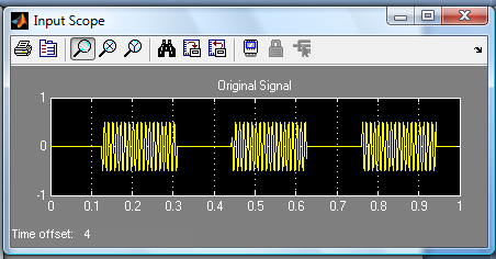
The waveform of voltage at the Input

The waveform of voltage at the cathode of both diodes i.e. Output voltage


The waveform of voltage across the inductor

Abstract:

Digital signal processing is the fundamental building block of modern digital developments. All types of digital innovations have been possible due to DSP. One of the first and most widely used application of digital signal processing is in the field of modern digital communication means. Due to exact linear phase it has become possible for engineers to design more reliable systems. DSP has deep impacts on modern communication systems. A general DSP processor simply performs functions of addition, multiplication and delay with necessary repetition.


Introduction:

Digital signal processing is extensively used in modern digital applications. As compared to analog signal processing, DSP serves us many benefits like phase linearization, easy storage, fast signal processing, cost effective, low frequency operation and general usage for any type of application. It has revolutionized the modern wired and wireless communication systems. Since a DSP processor simply perform repeated addition, multiplication and delay operations  during processing of information, so in this project we have demonstrated these basic operations by implementing them in MATLAB.

Objectives of the Project:

  • To learn the basic operation sequence of DSP processor.
  • Algorithmic approach to implement DSP basic operations.
  • A generalized MATLAB based implementation.

Sample Run:

%%%%%%%%%%%%%%%%%% DIGITAL SIGNAL PROCESSING PROJECT %%%%%%%%%%%%%%%
%%%%%%%%%%%%%%%%%%%% SOFTWARE IMPLEMENTATION OF %%%%%%%%%%%%%%%%%%%%
%%%%%%%%%%%%%%% DIGITAL SIGNAL PROCESSOR USING MATLAB %%%%%%%%%%%%%%
%%%%%%%%%%%%%%%%%%%%%%%%%%%%%%%%%%%%%%%%%%%%%%%%%%%%%%%%%%%%%%%%%%
%%%%%%%%%%%%%%%%%%%%%%%%%%%%%%%%%%%%%%%%%%%%%%%%%%%%%%%%%%%%%%%%%%
PROJECT BY:
IRZAM SHAHID
ANSAR SHARIF
M.NAEEM KHAN
FAHAD SABAH
%%%%%%%%%%%%%%%%%%%%%%%%%%%%%%%%%%%%%%%%%%%%%%%%%%%%%%%%%%%%%%%%%%
%%%%%%%%%%%%%%%%%%%%%%%%%%%%%%%%%%%%%%%%%%%%%%%%%%%%%%%%%%%%%%%%%%

T1 =

Columns 1 through 15

0     1     2     3     4     5     6     7     8     9    10    11    12    13    14

Columns 16 through 30

15    16    17    18    19    20    21    22    23    24    25    26    27    28    29

Columns 31 through 45

30    31    32    33    34    35    36    37    38    39    40    41    42    43    44

Columns 46 through 51

45    46    47    48    49    50

T2 =

Columns 1 through 15

0     1     2     3     4     5     6     7     8     9    10    11    12    13    14

Columns 16 through 30

15    16    17    18    19    20    21    22    23    24    25    26    27    28    29

Columns 31 through 45

30    31    32    33    34    35    36    37    38    39    40    41    42    43    44

Columns 46 through 51

45    46    47    48    49    50

Please enter delay…


For simulation code click the link given below

Download attachment

Envelope Detection

This demo implements two common methods of envelope detection and tests them with a sample speech signal and a modulated sine wave.

The envelope of a signal is the outline of the signal. It can be think of an envelope detector as a system that connects all of the peaks in the signal. Envelope detection has numerous applications in Signal Processing and Communications, including amplitude modulation (AM) detection.

Method 1: Squaring and Low Pass-Filtering


Method 2: The Hilbert Transform

Squaring and Low Pass-Filtering

The first method works by squaring the input signal and sending it through a low-pass filter. Squaring the signal effectively demodulates the input by using itself as the carrier wave. This means that half the energy of the signal is pushed up to higher frequencies and half is shifted towards DC. The envelope can then be extracted by keeping all the DC low-frequency energy and eliminating the high-frequency energy. In this demo, a simple minimum-phase low-pass filter is used to get rid of the high-frequency energy.

In order to maintain the correct scale, two more operations are included. The first is to place a gain of 2 on the signal. Since we are only keeping the lower half of the signal energy, this gain boosts the final energy to match its original energy. Finally, the square root of the signal is taken to reverse the scaling distortion from squaring the signal.

This method is useful because it is very easy to implement and can be done with a low-order filter, minimizing the lag of the output.

Method 2: The Hilbert Transform

The second method works by creating the analytic signal of the input by using a Hilbert transformer. An analytic signal is a complex signal, where the real part is the original signal and the imaginary part is the Hilbert transform of the original signal.

The Hilbert transform of the signal is found using a 32-point Parks-McClellan FIR filter. The Hilbert transform of the signal is then multiplied by i (the imaginary unit) and added to the original signal. The original signal is time-delayed before being added to the Hilbert transform to match the delay caused by the Hilbert transform, which is one-half the length of the Hilbert filter.

The envelope of the signal can be found by taking the absolute value of the analytic signal. In order to eliminate ringing and smooth the envelope, the result is subjected to a low-pass filter.

Envelope Detector Model

The all-platform floating-point version of the model is shown below. When we run the demo, we will see the original signal and the results of both envelope detectors.

Envelope Detector Results

This demo shows the results of the two different envelope detectors for two different types of input signals. The input choices are a sample speech signal or a 100 Hz sine wave that turns on and off.

The model has a switchable input and two outputs which are routed to scopes for easy viewing. If a signal is not visible, double-click on the Scope block to open it.

The input scope plot shows the original signal. The signal lasts a total of 5 seconds, with 1 second of data being shown at a time.


The first output scope plot shows the output of the first envelope detector. This is the result of squaring the original signal and sending it through a low-pass filter. You can clearly see that the envelope was successfully extracted from the speech signal.

The second output scope plot shows the output of the second envelope detector, which employs a Hilbert transform. Though the output of this envelope detector looks very similar to the first method.


For Simulink model and the block diagram of the above project click the link below:

Download attachment

Sample and Hold

Sample and hold circuit is the first step in the process of analog to digital conversion. It actually takes samples of the analog signal at specific time intervals depending on the clock frequency. Clock frequency is the frequency at which we are taking samples of the analog signal. Basically sample and hold process comprises of two steps:

  1. Take samples
  2. Holding samples


Samples are taken at the clock frequency while the hold step is accomplished by connecting the capacitor in the parallel to the output of the sampled signal. The simple sample and hold circuit is given below


The switch is on whenever we want to take sample and capacitor helps to hold that sample. Practrically the switch is implemented by connecting the fast switching FET switch, and samples are taken on some clock frequency which can be implemented by any timer circuit. The capacitor is invariably discharged by its own leakage current.


In our project we are taking audio signal frequency as the input signal. for sampling the input signal we must have sampling frequency twice of the bandwidth of the input signal. This is given by the sampling theorem. This theorem states that the sampling frequency must be the twice of the bandwidth of the input signal. If the sampling frequency is below the twice of the input signal bandwidth then aliasing of the samples will occur. Aliasing refers to an effect that causes different signals to become indistinguishable when sampled. The aliasing if the samples can be observe by taking the Fourier transform of the samples or by viewing the samples in the frequency domain. The higher the sample rate the more accurate the analog information will be in digital form and so the bandwidth. The higher sample rate has higher accuracy. The aliasing of the samples are describes in the figure given below

Components used in the project are as following:-

JFET BF245C:

The JFET BF245C is the simplest type of field effect transistor. It can be used as an

electronically-controlled switch or as a voltage-controlled resistance. Electric charge flows through a semiconducting channel between “source” and “drain” terminals. By applying a bias voltage to a “gate” terminal, the channel is “pinched”, so that the electric current is impeded or switched off completely.


Diode

Capacitors

Resistance

Power Supply

Function Generator:

The sampling clock is given to the gate channel of the JFET by the function generator or any timer circuit. The sampling frequency has its limitation which is describe by the sampling theorem.


Output waveform:

The output waveform of the simulation of sample and hold circuit is given below:


To download the circuit diagram click the link given below


Download attachment


Introduction

Here we are designing and implementing the four way traffic control system using  TTL logic.

There are different variations of traffic control. The most common ones that are seen are signs (board), road lines, islands (division between opposite lanes of vehicles), and traffic lights. The first one mentioned is easily understandable. Human sight translates a drawn sign, understands what it means and thus follows it. The second one, road lines, is also uncomplicated. A road line demarcates or delineates the allowable areas and lanes that a vehicle can occupy. And a road line shows where a car cannot go, cannot make a U-turn or overtake another vehicle. Islands do the same things.

Now a days due to ever increasing vehicles on the road, it require a efficient control on the four way junction of road. In order to find a solution to this problem the concept of an automatic traffic controller is conceived. Apart from providing efficient control of traffic, it also eliminate chance of human errors since it function automatically.

Features:

Traffic lights involve a rather complicated automated system that relies on sensors and programs. There are basically two types: the first type of traffic light has fixed time. That means, the green light may be on for a minute and off for the next few minutes while the rest of the traffic lights turn green. There is a fixed time for every street meeting at an intersection. And there is the variable type of traffic light. The variable type of traffic light relies on sensors underground that detect the flow of traffic approaching the intersection. If traffic is heavy, the green light stays longer than it would if the traffic were light. Coupled with the traffic light are the speed detector and the red light running detector. The speed detector uses a device that registers the speed of an oncoming vehicle. The latter, the red light running detector uses cameras that capture vehicles’ plates as they cross an intersection. The addition of this device was due to the rise in the number of crashes that occurred because of drivers beating the stoplight.

Basic Implementation:

The basic implementation of this project is:

1. The automatic traffic controller automatically switches on the four way junction for 8 seconds for direction control.

2. The main circuit components used are 555-Timer and 4-bit binary synchronous counter (74160).

3. The 555-Timer generates a clock signal for 8 seconds. This signal is used to clock counter circuit.

4. Binary counter is converted to 3 bit–counter to achieve 8 possible cases. The traffic light control is done by different Boolean function of logic gate.

Project Report

Datasheets:

74LS160

555 Timer IC

7404

7432

7408

7411

Circuit Diagram:


Download attachment

Overview

Abstract:

To develop  DIGITAL CLOCK using 7 segment display. It show hours and  minutes. Make it by using discrete components.

Introduction:

A digital clock is a type of clock that displays the time digitally. Digital clocks are often associated with electronic drives, but the “digital” description refers only to the display, not to the drive mechanism.

Basically a digital clock requires these basic elements or blocks

  • A source of power to run the clock
  • An accurate timebase that acts as the clock’s heartbeat
  • A way to gear down the timebase to extract different components of time (hours, minutes, seconds).

A way to display the time

WORKING OVERVIEW:

At the heart of the clock there is a piece that can generate an accurate 60-hertz (Hz, oscillations per second) signal. There are two ways to generate this signal:

  1. The signal can be extracted from the 60-Hz oscillations in a normal power line. Many clocks that get their power from a wall socket use this technique because it is cheap and easy. The 60-Hz signal on the power line is reasonably accurate for this purpose.
  1. The signal can be generated using a crystal oscillator. Obviously, any battery-operated clock or wristwatch will use this technique instead. It takes more parts, but is generally much more accurate.

The 60-Hz signal is divided down using a counter. A typical TTL part to use is a decade counter. This part can be configured to divide by any number between 2 and 10, and generates a binary number as output. So we take our 60-Hz time base, divide it by 10, divide it by 6 and now we have a 1-Hz (1 oscillation per second) signal. This 1-Hz signal is perfect for driving the “second hand” portion of the display. Similarly by configuring the decade counter we can produce the minute hand and hour hand also.

To actually see the output of the counters we need to drive a display. The two counters produce binary numbers. The divide-by-10 counter is producing a 0-1-2-3-4-5-6-7-8-9 sequence on its outputs, while the divide-by-6 counter is producing a 0-1-2-3-4-5 sequence on its outputs.

We want to display these binary numbers on something called a 7-segment display. A 7-segment display has seven bars on it, and by turning on different bars we can display different numbers. To convert a binary number between 0 and 9 to the appropriate signals to drive a 7-segment display, we use a “binary number to 7-segment display converter.” This chip looks at the binary number coming in and turns on the appropriate bars in the 7-segment LED to display that number.

Project Report:

Datasheets:

74LS160

74LS10

74LS20

74LS47

555 Timer IC

Circuit Diagram:

Download attachment