electronics

Every year GIKI offers admissions in Undergraduate Engineering programs. Here we will provide info about GIKI Undergraduate Admissions 2013 including prospectus, application process, GIKI Entry Test 2013, GIKI undergraduate merit lists and all other aspects of admission. Note that we are only facilitating students with the admission information, all the admission process will be dealt with the University itself. Thousands of intermediate students from all over the Pakistan apply for admissions every year in undergraduate engineering programs of Ghulam Ishaq Khan Institute. GIKI is one of the top most engineering institute of Pakistan.

GIKI Admissions 2013 Procedure Overview

GIKI announces its undergraduate admissions in April or May of every year. This year the admission process will start from 28th April 2013 with the availability of Prospectus. Then the online form submission for admissions will start from 28th April 2013. The last date for the admission submission is 20th June 2013. After the last date of form submission GIKI will provide the admit cards for the Admission test (GIKI Entry Test 2013). The entry test will held on 7th July 2013. After that Admission test result will be announced and merit lists will be displayed. The admitted candidates will then start their first semester on 26th August 2013.

GIKI Application Procedure

  • Create an account (register yourself) .  https://admission.giki.edu.pk
  • Login and submit online application form
  • Prepare a package of the following documents:
  • Admit Card (printed online)
  • Application Form (printed online)
  • Optional Scholarship Form (printed online)
  • Proof of payment: Rs. 2500 (for local) + Rs. 500 (if applying for financial assistance) / US $170 (overseas)
  • Photocopies of Academic Documents
  • Two additional passport size photographs
  • Send the above documents (in Single package) at the address given as below:

Undergraduate Admission Office
GIK Institute of Engineering Sciences & Technology
Khyber Pakhtunkwa, Pakistan
Ph: +92-938-271440
Cell: +92-334-8696119

  • How to pay the Application Processing fee ?

Processing fee can be paid:
Online to HBL A/C No. 19790000085901 for payment in PKR
OR
For payment in US $:
Bank: Habib Bank Ltd
Title of Account: GIK Institute Topi
Account No: 19790002044611
Branch Code: 1979
Swift Code: HABB PKK AXXX

  • To send your SAT-II Score, use GIK Institute’s registered Institute Code: 0096

GIKI UG Admission Schedule

Event

Date

Availability of Prospectus – Class of 2017

Apr 28, 2013

Online Submission of Admission Form Starts

Apr 28, 2013

Online Submission of Admission Form Ends

Jun 20, 2013

Last date for receipt of documents

Jun 23, 2013

Admission Test

Jul 07, 2013

Last date for receipt of SAT- II Scores (overseas applicants)

Jul 08, 2013

Induction Ceremony

Aug 24, 2013

Semester Starts

Aug 26, 2013

GIKI Entry Test 2013

GIKI offers admissions on the basis of candidate’s earlier academic background and the score of the Admission test conducted by GIKI. This admission test is also known as GIKI Entry Test. This admission test is very important and the admission of the candidate mostky depends on the score of this admission test. the weight-age of this admission test in the selection process is 85%. For more information about the GIKI Entry test and its pattern and sample test paper, visit the link given below.

Click GIKI Entry Test 2013 for details

Click GIKI Entry Test Result 2013 to check result

Undergraduate Programs

GIKI offers admissions in the following undergraduate programs:

  • Computer Science and Engineering
  • Electronic Engineering
  • Chemical Engineering (Newly announced Undergraduate program)
  • Electrical Engineering (Power) (Newly announced Undergraduate program)
  • Engineering Sciences
  • Humanities & Management Sciences
  • Mechanical Engineering
  • Metallurgy & Materials Engineering/ Material Science and Engineering
  • Mathematics
  • Physics
  • Bachelor in Management Sciences (Newly announced Undergraduate program)

Basic Eligibility Criteria


Basic Eligibility for Engineering and Computer Science Programs

1. HSSC (Pre-Engineering i.e Mathematics, Physics and Chemistry)

2. HSSC (Pre-Medical) with Additional Mathematics

3. Three A-level in Mathematics, Physics and Chemistry and O-level in eight subjects (English, Mathematics, Physics, Chemistry, Biology/Computer Science, Urdu, Islamic Studies & Pakistan Studies) for local applicants and in five required subjects for those applying from abroad.

4. American or Canadian High School Diploma or International Baccalaureate Diploma with Mathematics (with Calculus), Physics and Chemistry

5. B.Sc. (Mathematics & Physics)

6. Three year Diploma of Associate Engineering (DAE) in relevant technology from a Pakistani Board of Technical Education

60% marks or Equivalent Grades in Mathematics, Physics and Overall

Note: Applicant with Mathematics, Physics and Chemistry background can apply for all programs however those having studied Computer Science / Computer Studies in lieu of Chemistry at their HSSC or A-levels, can only apply for Computer Engineering or Computer Science.
Basic Eligibility Management Science Program

1. HSSC (Pre-Engg), HSSC (General Science), HSSC (ICS), HSSC (Pre-Medical) with Additional Mathematics

2. A-Level in three subjects and O-Level in eight subjects for local OR O-Level in five subjects for those applying from abroad

3. American or Canadian High School Diploma or International Baccalaureate Diploma


60% Marks or Equivalent grades
Comparative Assessment (Merit List) CriterionScore in Admission Test   OR  SAT II in Mathematics and Physics for those applying from outside Pakistan (For Engineering and Computer Science Programs)Score in GCAT (GIKI Common Admission Test) OR  SAT for those applying from outside Pakistan (For Management  Science Program


SSC/Equivalent  + HSSC Part I

O-level (for those with A- and O-level background)

Last completed qualification for IB diploma or B.Sc. or DAE

Weightage85% 

85%


5% + 10%

15%

15%

GIKI UG Admissions Contact Info

Phone No. NWD : 0938-271440
Cell # 0334-8696119, 0303-5394528
Email: [email protected]

Further information about the GIKI Admissions 2013 will be updated soon. The eligibility criteria, selection procedure, Scholarship and loans information will be avialable soon, so stay with us and keep visiting us. We will keep you up to date with the GIKI admission process.

If students have any queries regarding GIKI admissions, they can ask us by commenting below in the comment section. We will utterly try to help them. Don;t forget to share this admission news with your friends; you can share this by clicking the sharing buttons given below.

Click Engineering Admissions 2013 for other university’s admissions

Abstract

One of the first and most widely used application of power electronic devices have been in rectification. Rectification refers to the process of converting an ac voltage or current source to dc voltage and current. Rectifiers specially refer to power electronic converters where the electrical power flows from the ac side to the dc side. In many situations the same converter circuit may carry electrical power from the dc side to the ac side where upon they are referred to as inverters. We will be Designing and Simulating single phase half wave Rectifier; commonly used rectifier circuits supplying different types of loads (resistive, inductive, capacitive, back emf type) will be presented.

Contents

  • Introduction……………………………………………
  • Objectives of the Project…………………………..
  • Point of interests
  • Circuit Description & Operation………………..
  • Mathematical Analysis…………………………….
  • Computer simulation
    • Software Code
    • Sample Run
    • Outputs
      • Circuit
      • Outputs
      • Block Diagram
      • Outputs

1.      MATLAB Simulation

2.      MATLAB Simulink (Time Domain Implementation)

3.      MATLAB Simulink (Frequency Domain Implementation)

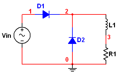
4.      Multisim Implementation…………………………


Introduction

Single phase rectifiers are extensively used in a number of power electronic based converters. In most cases they are used to provide an intermediate unregulated dc voltage source which is further processed to obtain a regulated dc or ac output. They have, in general, been proved to be efficient.


Objectives of the Project:

  • Analyze the operation of single phase half wave rectifier supply resistive, inductive loads.
  • Define and calculate the Performance Parameters of the rectifier.
  • Simulate the circuit with computer software package (MATLAB)
  • In addition to MATLAB we also simulated the project in Multisim


Points of interest in the analysis will be.

•   Waveforms and characteristic values (average, RMS etc) of the rectified voltage and current.

•   Influence of the load type on the rectified voltage and current.

•   Reaction of the rectifier circuit upon the ac network, reactive power requirement, power factor, harmonics etc.

Circuit Description & Operation:

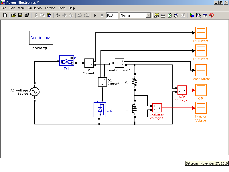
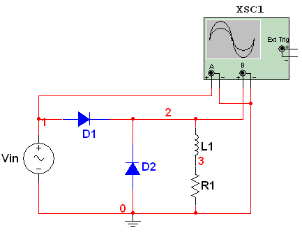
Let the source voltage vs be defined to be E*sin (wt). The source voltage is positive when 0 < wt < pi  radians and it is negative when pi < wt < 2 pi radians. When vs is positive, diode D1 conducts and the voltage vc is positive. This in turn leads to diode D2 being reverse-biased during this period. During  pi < wt < 2 pi the voltage vc would be negative if diode D1 tends to conduct. This means that D2 would be forward-biased and would conduct. When diode D2 conducts, the voltage vc would be zero volts, assuming that the diode drop is negligible. Additionally when diode D2 conducts, diode D1 remains reverse-biased, because the voltage vs is negative. When the current through the inductor tends to fall, it starts acting as a source. When the inductor acts as a source, its voltage tends to forward bias diode D2 if the source voltage vs is negative and forward bias diode D1 if the source voltage vs is positive. Even when the source voltage vs is positive, the inductor current would tend to fall if the source voltage is less than the voltage drop across the load resistor. During the negative half-cycle of source voltage, diode D1 blocks conduction and diode D2 is forced to conduct. Since diode D2 allows the inductor current circulate through L, R and D2, diode D2 is called the free-wheeling diode. We can say that the current free-wheels through D2.

Mathematical Analysis

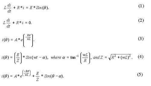
An expression for the current through the load can be obtained as shown below. It can be assumed that the load current flows all the time. In other words, the load current is continuous. When diode D1 conducts, the driving function for the differential equation is the sinusoidal function defining the source voltage. During the period defined by pi < wt < 2pi, diode D1 blocks current and acts as an open switch. On the other hand, diode D2 conducts during this period, the driving function can be set to be zero volts. For 0 < wt <pi, the equation (1) shown below applies.

For the negative half-cycle of the source, equation (2) applies. As in the previous case, the solution is obtained in two parts. The expressions for the complementary integral and the particular integral are the same. The expression for the complementary integral is presented by equation (3). The particular solution to the equation (1) is the steady-state response and is presented as equation (4). The total solution is the sum of both the complimentary and the particular solution. The total solution is presented as equation (5).

The difference in solution is in how the constant A in complementary integral is evaluated. In the case of the circuit without free-wheeling diode, i(0) = 0, since the current starts building up from zero at the start of every positive half-cycle. On the other hand, the current-flow is continuous when the circuit contains a free-wheeling diode also. Since the input to the RL circuit is a periodic half-sinusoid function, we expect that the response of the circuit should also be periodic. That means, the current through the load is periodic. It means that i(0) = i(2).

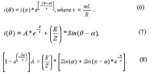
Since the current through the load free-wheels during  <  < 2, we get equation (6). We use ( -  ) for the elapsed period in radians instead of  itself, since the free-wheeling action starts at  =  . From the total solution, we can get i() from equation (7) by substituting  = . To obtain A, the following steps are necessary. From the total solution, obtain an expression for i(0) by substituting 0 for . Also obtain an expression for i() by substituting  for in equation (7). Using this expression for i() in equation (6), obtain i(2) by letting  = 2 . Since i(0) = i(2), we can obtain A from equation (8). In equation (8), the terms containing constant A are grouped on the left-hand side of equation and the other terms on the right-hand side.

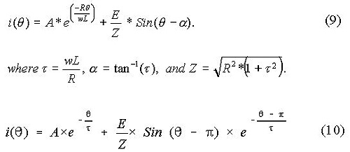
The operation of the circuit can be simulated as shown below. During 0 <  <  , the expression for current is presented as equation (9). During  <  < 2 , the expression for current is shown as equation (10).

Computer simulation

We simulated the project using various computer simulation techniques, the soft form is also provided

MATLAB Simulation

Software Code:

%PROJECT TITLE:

%DESIGN AND IMPLEMENTATION OF HALF WAVE RECTIFIER

disp(‘%%%%%%%%%%%%%%%%%% POWER ELECTRONICS PROJECT %%%%%%%%%%%%%%%%%%%%%’);

disp(‘%%%%%%%%%%%%%%%%% DESIGN AND IMPLEMENTATION OF %%%%%%%%%%%%%%%%%%%’);

disp(‘%%%%%%%%%%%%%%% SINGLE PHASE HALF WAVE RECTIFIER %%%%%%%%%%%%%%%%%’);

disp(‘%%%%%%%%%%%%%%%%%%%%%%%%%%%%%%%%%%%%%%%%%%%%%%%%%%%%%%%%%%%%%%%%%%’);

disp(‘%%%%%%%%%%%%%%%%%%%%%%%%%%%%%%%%%%%%%%%%%%%%%%%%%%%%%%%%%%%%%%%%%%’);

disp(‘%%%%%%%%%%%%%%%%%%%%%%%%%%%%%%%%%%%%%%%%%%%%%%%%%%%%%%%%%%%%%%%%%%’);

disp(‘%%%%%%%%%%%%%%%%%%%%%%%%%%%%%%%%%%%%%%%%%%%%%%%%%%%%%%%%%%%%%%%%%%’);

disp(‘ENTER REQUIRED DESIGN PARAMETERS…’)

%PEAK VOLTAGE: Vp IN VOLTS

peakV=input(‘ENTER PEAK VOLTAGE IN VOLTS: ‘);

%CIRCUIT OPERATI0N FREQUENCY freq (Hz)

freq=input(‘ENTER OPERATING FREQUENCY IN Hz: ‘);

%LOAD INDUCTANCE L(mH)

L=input(‘ENTER LOAD INDUCTANCE IN mH: ‘);

%LOAD RESISTANCE R(Ohms)

R=input(‘ENTER LOAD RESISTANCE IN ohm: ‘);

%Setting the required parameters

w=2.0*pi*freq;

angle=atan(w*L/R);

Idc =0.318*peakV/R;

Vdc=0.318*peakV;

X=w*L/1000.0;

if (X<0.001) X=0.001; end;

Z=sqrt(R*R+X*X);

tauInv=R/X;

loadAng=atan(X/R);

A1=peakV/Z*sin(loadAng);

A2=peakV/Z*sin(pi-loadAng)*exp(-pi*tauInv);

A3=(A1+A2)/(1-exp(-2.0*pi*tauInv));

Ampavg=0;

AmpRMS=0;

dccur =0;

dcvolt=0;

Pdc = 0;

for n=1:360;

theta=n/180.0*pi;

X(n)=n;

if (n<180)

cur=peakV/Z*sin(theta-loadAng)+A3*exp(-tauInv*theta);

Ampavg=Ampavg+cur*1/360;

AmpRMS=AmpRMS+cur*cur*1/360;

else

A4=peakV/Z*sin(pi-loadAng)*exp(-(theta-pi)*tauInv);

cur=A4+A3*exp(-tauInv*theta);

Ampavg=Ampavg+cur*1/360;

AmpRMS=AmpRMS+cur*cur*1/360;

end;

if (n<180)

Vind(n)=peakV*sin(theta)-R*cur;

Vout(n)=peakV*sin(theta);

diode2cur(n)=0;

diode1cur(n)=cur;

dcvolt = sqrt(Vout(n))/2;

else

Vind(n)=-R*cur;

Vout(n)=0;

diode2cur(n)=cur;

diode1cur(n)=0;

end

Vrms=peakV/2;

Irms=Vrms/R;

Is1=Irms;

iLoad(n)=cur;

dccur = sqrt(iLoad(n))/2;

end;

disp(‘SINGLE PHASE HALF WAVE RECTIFIER PERFORMANCE PARAMETERS’);

Pdc = Vdc*Idc;

disp(‘1: The Average DC Power is…’);

disp(Pdc);

Pac = Vrms*Irms;

disp(‘2: The Average AC Power is…’);

disp(Pac);

eff=Pdc/Pac;

disp(‘3: THE PERCENTAGE RECTIFICATION RATIO OF THE RECTIFIER…’);

disp(eff);

Vac=sqrt(Vrms^2-Vdc^2);

disp(‘4: The Effective Value Of AC Componenet of Output Voltage is…’);

disp(Vac);

FF=Vrms/Vdc;

disp(‘5: The Form Factor is…’);

disp(FF);

RF=Vac/Vdc;

disp(‘6: The Ripple Factor is…’);

disp(RF);

TUF=Pdc/(Vrms*Irms);

disp(‘7: The Transformer Utilization Factor is…’);

disp(TUF);

DF=cos(angle);

disp(‘8: The Displacement Factor is…’);

disp(DF);

HF=sqrt((Irms/Is1)-1);

disp(‘9: The Harmonic Factor is…’);

disp(HF);

PF=(Is1/Irms)*cos(angle);

disp(’10: The Power Factor is…’);

disp(PF);

CF=peakV/(R*Irms);

disp(’11: The Crest Factor is…’);

disp(CF);

%Plotting Corresponding input and Output Currents and Voltages

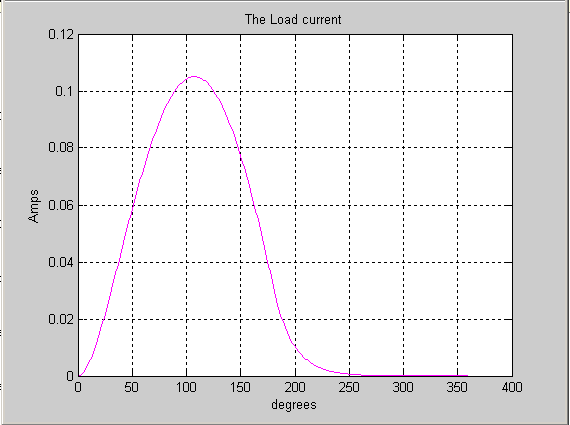
plot(X,iLoad,’m’)

title(‘The Load current’)

xlabel(‘degrees’)

ylabel(‘Amps’)

grid

pause

plot(X,Vout,’r’)

title(‘Voltage at cathode’)

xlabel(‘degrees’)

ylabel(‘Volts’)

grid

pause

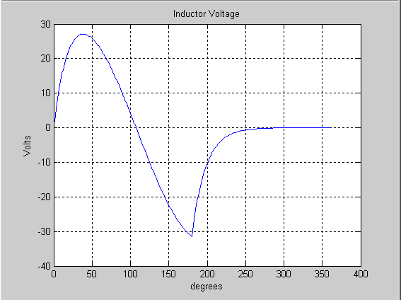
plot(X,Vind,’b’)

title(‘Inductor Voltage’)

xlabel(‘degrees’)

ylabel(‘Volts’)

grid

pause

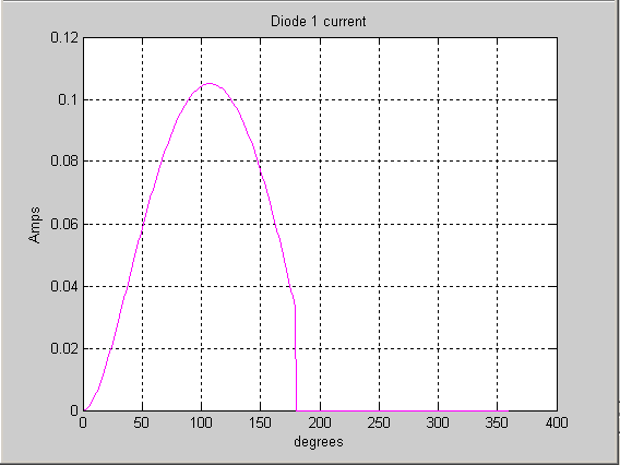
plot(X,diode1cur,’m’)

title(‘Diode 1 current’)

xlabel(‘degrees’)

ylabel(‘Amps’)

grid

pause

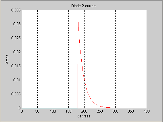
plot(X,diode2cur,’r’)

title(‘Diode 2 current’)

xlabel(‘degrees’)

ylabel(‘Amps’)

grid

Sample Run:

%%%%%%%%%%%%%%% POWER ELECTRONICS PROJECT %%%%%%%%%%%%%%%%%%

%%%%%%%%%%%%%%% DESIGN AND IMPLEMENTATION OF %%%%%%%%%%%%%%%

%%%%%%%%%%%%% SINGLE PHASE HALF WAVE RECTIFIER %%%%%%%%%%%%%

%%%%%%%%%%%%%%%%%%%%%%%%%%%%%%%%%%%%%%%%%%%%%%%%%%%%%%%%%%%%

%%%%%%%%%%%%%%%%%%%%%%%%%%%%%%%%%%%%%%%%%%%%%%%%%%%%%%%%%%%%

%%%%%%%%%%%%%%%%%%%%%%%%%%%%%%%%%%%%%%%%%%%%%%%%%%%%%%%%%%%%

%%%%%%%%%%%%%%%%%%%%%%%%%%%%%%%%%%%%%%%%%%%%%%%%%%%%%%%%%%%%

ENTER REQUIRED DESIGN PARAMETERS…

ENTER PEAK VOLTAGE IN VOLTS: 110

ENTER OPERATING FREQUENCY IN Hz: 50

ENTER LOAD INDUCTANCE IN mH: 1000

ENTER LOAD RESISTANCE IN ohm: 1000


%%%%%%%%%%%%%%%%%%%%%%%%%%% OUTPUT %%%%%%%%%%%%%%%%%%%%%%%%%%%%%%%

SINGLE PHASE HALF WAVE CONTROLLED RECTIFIER PERFORMANCE PARAMETERS

%%%%%%%%%%%%%%%%%%%%%%%%%%%%%%%%%%%%%%%%%%%%%%%%%%%%%%%%%%%%%%%%%%

1: The Average DC Power is…

1.2236


2: The Average AC Power is…

3.0250


3: The Efficiency Of Rectifier is…

0.4045


4: The Effective Value Of AC Componenet of Output Voltage is…

42.4429


5: The Form Factor is…

1.5723


6: The Ripple Factor is…

1.2133


7: The Transformer Utilization Factor is…

0.4045


8: The Displacement Factor is…

0.0032


9: The Harmonic Factor is…

0


10: The Power Factor is…

0.0032


11: The Crest Factor is…

2


OUTPUTS:

The Voltage waveform at output or at the cathodes of both the diodes:

The current waveform at output or Load current:

The voltage waveform across the inductor:

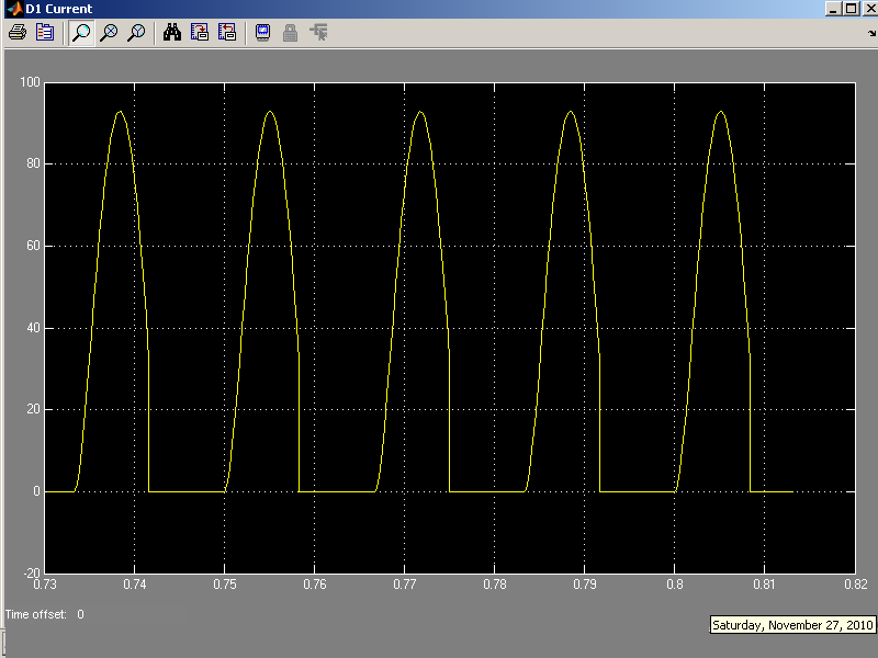
Diode1 current waveform:

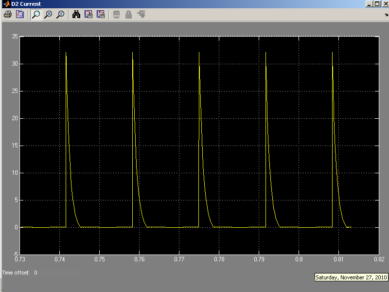
Diode2 current waveform:

MATLAB Simulink (Time Domain Implementation)

Following is the Matlab Simulink Implementation in time domain:


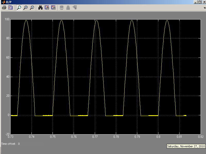
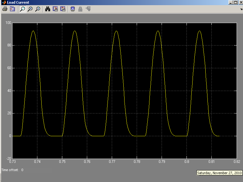
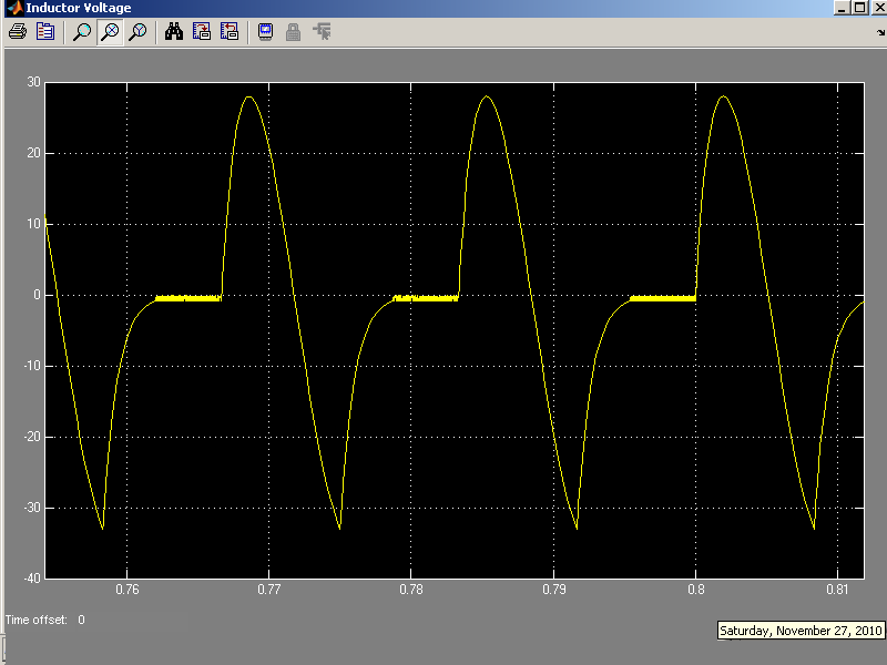
OUTPUTS:

The Voltage waveform at output or at the cathodes of both the diodes

The current waveform at output or Load current

The voltage waveform across the inductor

Diode1 current waveform

Diode2 current waveform

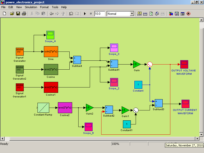
MATLAB Simulink(Frequency Domain)

Following is the Matlab Simulink Implementation in Frequency domain:

Output Voltage Waveform
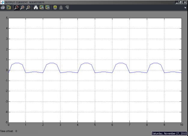
Output Current Waveform

MULTISIM Implementation:


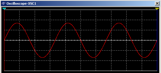
The waveform of voltage at the Input

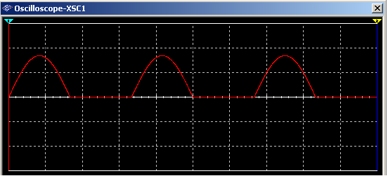
The waveform of voltage at the cathode of both diodes i.e. Output voltage


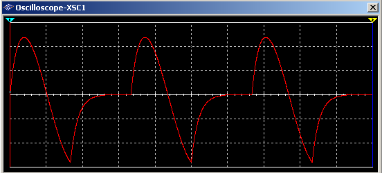
The waveform of voltage across the inductor

Abstract:

Digital signal processing is the fundamental building block of modern digital developments. All types of digital innovations have been possible due to DSP. One of the first and most widely used application of digital signal processing is in the field of modern digital communication means. Due to exact linear phase it has become possible for engineers to design more reliable systems. DSP has deep impacts on modern communication systems. A general DSP processor simply performs functions of addition, multiplication and delay with necessary repetition.


Introduction:

Digital signal processing is extensively used in modern digital applications. As compared to analog signal processing, DSP serves us many benefits like phase linearization, easy storage, fast signal processing, cost effective, low frequency operation and general usage for any type of application. It has revolutionized the modern wired and wireless communication systems. Since a DSP processor simply perform repeated addition, multiplication and delay operations  during processing of information, so in this project we have demonstrated these basic operations by implementing them in MATLAB.

Objectives of the Project:

  • To learn the basic operation sequence of DSP processor.
  • Algorithmic approach to implement DSP basic operations.
  • A generalized MATLAB based implementation.

Sample Run:

%%%%%%%%%%%%%%%%%% DIGITAL SIGNAL PROCESSING PROJECT %%%%%%%%%%%%%%%
%%%%%%%%%%%%%%%%%%%% SOFTWARE IMPLEMENTATION OF %%%%%%%%%%%%%%%%%%%%
%%%%%%%%%%%%%%% DIGITAL SIGNAL PROCESSOR USING MATLAB %%%%%%%%%%%%%%
%%%%%%%%%%%%%%%%%%%%%%%%%%%%%%%%%%%%%%%%%%%%%%%%%%%%%%%%%%%%%%%%%%
%%%%%%%%%%%%%%%%%%%%%%%%%%%%%%%%%%%%%%%%%%%%%%%%%%%%%%%%%%%%%%%%%%
PROJECT BY:
IRZAM SHAHID
ANSAR SHARIF
M.NAEEM KHAN
FAHAD SABAH
%%%%%%%%%%%%%%%%%%%%%%%%%%%%%%%%%%%%%%%%%%%%%%%%%%%%%%%%%%%%%%%%%%
%%%%%%%%%%%%%%%%%%%%%%%%%%%%%%%%%%%%%%%%%%%%%%%%%%%%%%%%%%%%%%%%%%

T1 =

Columns 1 through 15

0     1     2     3     4     5     6     7     8     9    10    11    12    13    14

Columns 16 through 30

15    16    17    18    19    20    21    22    23    24    25    26    27    28    29

Columns 31 through 45

30    31    32    33    34    35    36    37    38    39    40    41    42    43    44

Columns 46 through 51

45    46    47    48    49    50

T2 =

Columns 1 through 15

0     1     2     3     4     5     6     7     8     9    10    11    12    13    14

Columns 16 through 30

15    16    17    18    19    20    21    22    23    24    25    26    27    28    29

Columns 31 through 45

30    31    32    33    34    35    36    37    38    39    40    41    42    43    44

Columns 46 through 51

45    46    47    48    49    50

Please enter delay…


For simulation code click the link given below

Download attachment

Sample and Hold

Sample and hold circuit is the first step in the process of analog to digital conversion. It actually takes samples of the analog signal at specific time intervals depending on the clock frequency. Clock frequency is the frequency at which we are taking samples of the analog signal. Basically sample and hold process comprises of two steps:

  1. Take samples
  2. Holding samples


Samples are taken at the clock frequency while the hold step is accomplished by connecting the capacitor in the parallel to the output of the sampled signal. The simple sample and hold circuit is given below


The switch is on whenever we want to take sample and capacitor helps to hold that sample. Practrically the switch is implemented by connecting the fast switching FET switch, and samples are taken on some clock frequency which can be implemented by any timer circuit. The capacitor is invariably discharged by its own leakage current.


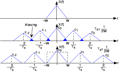
In our project we are taking audio signal frequency as the input signal. for sampling the input signal we must have sampling frequency twice of the bandwidth of the input signal. This is given by the sampling theorem. This theorem states that the sampling frequency must be the twice of the bandwidth of the input signal. If the sampling frequency is below the twice of the input signal bandwidth then aliasing of the samples will occur. Aliasing refers to an effect that causes different signals to become indistinguishable when sampled. The aliasing if the samples can be observe by taking the Fourier transform of the samples or by viewing the samples in the frequency domain. The higher the sample rate the more accurate the analog information will be in digital form and so the bandwidth. The higher sample rate has higher accuracy. The aliasing of the samples are describes in the figure given below

Components used in the project are as following:-

JFET BF245C:

The JFET BF245C is the simplest type of field effect transistor. It can be used as an

electronically-controlled switch or as a voltage-controlled resistance. Electric charge flows through a semiconducting channel between “source” and “drain” terminals. By applying a bias voltage to a “gate” terminal, the channel is “pinched”, so that the electric current is impeded or switched off completely.


Diode

Capacitors

Resistance

Power Supply

Function Generator:

The sampling clock is given to the gate channel of the JFET by the function generator or any timer circuit. The sampling frequency has its limitation which is describe by the sampling theorem.


Output waveform:

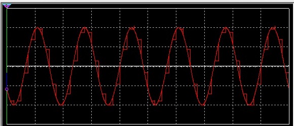
The output waveform of the simulation of sample and hold circuit is given below:


To download the circuit diagram click the link given below


Download attachment