Check 9th Class Date Sheet 2013 of all boards. 9th class (SSC part 1) annual exams 2013 date sheet of all groups including 9th class General, Science, Arts and Commerce group. Sometimes the 9th Date Sheet 2013 is also referred as SSC part 1 Date Sheet 2013 or Matric Part 1 Date Sheet 2013. SSC stands for Secondary School Certificate. All the education boards of Pakistan announces the 9th Class annual exam date sheet for 2013 examinations. 9th Class annual exams 2013 usually held in the month of February and March.
To find out the exact date of the 9th Class Exams 2013 and subject vise 9th Class Date Sheet 2013 of specific education board, click the board from the list given below. The subject vise detailed date sheet of that board will be given in its respective page.
Students of 9th Class are advised to keep themselves up to date with their board’s 9th Date Sheet 2012 for the better and early preparation of their exams. As it is important to know about the exam dates and make proper schedule to prepare for their exams.
For the help of the students we also facilitating them with the 9th Class Model Papers and Paper Pattern according to new/latest (2013) exam pattern.
The date sheet will be available on the respective pages of the boards and the links of these boards are given in the list above. On the announcement of the 9th class date sheet 2013 we will update the 9th date sheet 2013 on the respective page of the board. So stay with us and keep visiting us. We will keep you update about the 9th Class exams schedule 2013.
If students have any queries regarding 9th Class Date Sheet 2013, they can ask us commenting below in the comment section. We will utterly try to answer their question.
Don’t forget to share these important date sheets with your friends. You can share these date sheets by clicking the sharing buttons given below.
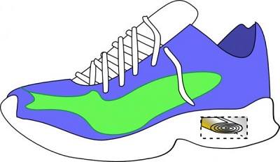
Illustration of Dr. Ville Kaajakari's shoe power generator. (Credit: Image courtesy of Louisiana Tech University)
Dr. Ville Kaajakari, assistant professor of electrical engineering at Louisiana Tech University has developed a technology that harvests power from a small generator embedded in the sole of a shoe.
Kaajakari’s innovative technology, developed at Louisiana Tech’s Institute for Micromanufacturing (IfM), is based on new voltage regulation circuits that efficiently convert a piezoelectric charge into usable voltage for charging batteries or for directly powering electronics.
“This technology could benefit, for example, hikers that need emergency location devices or beacons,” said Kaajakari. “For more general use, you can use it to power portable devices without wasteful batteries.”
The technology is being featured by MEMS Investor Journal, a national online industry publication. MEMS are tiny “smart” devices that combine computer chips with micro-components such as sensors, gears, flow-channels, mirrors and actuators.MEMS Investor Journal is an independent publication that provides investment professionals with the latest developments in the micro electro mechanical systems (MEMS) industry.
According to the article, energy harvesting is an attractive way to power MEMS sensors and locator devices such as GPS. However, power harvesting technologies often fall short in terms of output as many of today’s applications require higher power levels.
Kaajakari’s breakthrough uses a low-cost polymer transducer that has metalized surfaces for electrical contact. Unlike conventional ceramic transducers, the polymer-based generator is soft and robust, matching the properties of regular shoe fillings. The transducer can therefore replace the regular heel shock absorber with no loss in user experience.
In addition to running sensors and inertial navigation, Kaajakari’s shoe power generator can also be used to power RF transponders and GPS receivers.
“Ultimately, we want to bring up the power levels up to a point where we could, in addition to sensors, charge or power other portable devices such as cell phones.”
Article: Microstructured piezoelectric shoe power generator outperforms batteries
Story Source:
The above story is reprinted from materials provided by Louisiana Tech University. The original article was written by Dave Guerin.
In a just-published paper in the magazine Science, IBM researchers demonstrated a radio-frequency graphene transistor with the highest cut-off frequency achieved so far for any graphene device — 100 billion cycles/second (100 GigaHertz).
This accomplishment is a key milestone for the Carbon Electronics for RF Applications (CERA) program funded by DARPA, in an effort to develop next-generation communication devices.
The high frequency record was achieved using wafer-scale, epitaxially grown graphene using processing technology compatible to that used in advanced silicon device fabrication.
“A key advantage of graphene lies in the very high speeds in which electrons propagate, which is essential for achieving high-speed, high-performance next generation transistors,” said Dr. T.C. Chen, vice president, Science and Technology, IBM Research. “The breakthrough we are announcing demonstrates clearly that graphene can be utilized to produce high performance devices and integrated circuits.”
Graphene is a single atom-thick layer of carbon atoms bonded in a hexagonal honeycomb-like arrangement. This two-dimensional form of carbon has unique electrical, optical, mechanical and thermal properties and its technological applications are being explored intensely.
Uniform and high-quality graphene wafers were synthesized by thermal decomposition of a silicon carbide (SiC) substrate. The graphene transistor itself utilized a metal top-gate architecture and a novel gate insulator stack involving a polymer and a high dielectric constant oxide. The gate length was modest, 240 nanometers, leaving plenty of space for further optimization of its performance by scaling down the gate length.
It is noteworthy that the frequency performance of the graphene device already exceeds the cut-off frequency of state-of-the-art silicon transistors of the same gate length (~ 40 GigaHertz). Similar performance was obtained from devices based on graphene obtained from natural graphite, proving that high performance can be obtained from graphene of different origins. Previously, the team had demonstrated graphene transistors with a cut-off frequency of 26 GigaHertz using graphene flakes extracted from natural graphite.
Story Source:
The above story is reprinted from materials provided by IBM.
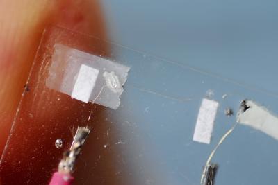
Close-up image shows a pair of entangled fibers that make up a microfiber nanogenerator. Both fibers are coated with zinc oxide nanowires; one fiber is additionally coated with gold. When rubbed together, they generate electrical current. (Credit: Georgia Tech Photo: Gary Meek)
Nanotechnology researchers are developing the perfect complement to the power tie: a “power shirt” able to generate electricity to power small electronic devices for soldiers in the field, hikers and others whose physical motion could be harnessed and converted to electrical energy.
The February 14 issue of the journal Nature details how pairs of textile fibers covered with zinc oxide nanowires can generate electrical current using the piezoelectric effect. Combining current flow from many fiber pairs woven into a shirt or jacket could allow the wearer’s body movement to power a range of portable electronic devices. The fibers could also be woven into curtains, tents or other structures to capture energy from wind motion, sound vibration or other mechanical energy.
“The fiber-based nanogenerator would be a simple and economical way to harvest energy from physical movement,” said Zhong Lin Wang, a Regents professor in the School of Materials Science and Engineering at the Georgia Institute of Technology. “If we can combine many of these fibers in double or triple layers in clothing, we could provide a flexible, foldable and wearable power source that, for example, would allow people to generate their own electrical current while walking.”
The microfiber-nanowire hybrid system builds on the nanowire nanogenerator that Wang’s research team announced in April 2007. That system generates current from arrays of vertically-aligned zinc oxide (ZnO) nanowires that flex beneath an electrode containing conductive platinum tips. The nanowire nanogenerator was designed to harness energy from environmental sources such as ultrasonic waves, mechanical vibrations or blood flow.
The nanogenerators developed by Wang’s research group take advantage of the unique coupled piezoelectric and semiconducting properties of zinc oxide nanostructures, which produce small electrical charges when they are flexed. After a year of development, the original nanogenerators — which are two by three millimeters square — can produce up to 800 nanoamperes and 20 millivolts.
The microfiber generators rely on the same principles, but are made from soft materials and designed to capture energy from low-frequency mechanical energy. They consist of DuPont Kevlar fibers on which zinc oxide nanowires have been grown radially and embedded in a polymer at their roots, creating what appear to be microscopic baby-bottle brushes with billions of bristles. One of the fibers in each pair is also coated with gold to serve as the electrode and to deflect the nanowire tips.
“The two fibers scrub together just like two bottle brushes with their bristles touching, and the piezoelectric-semiconductor process converts the mechanical motion into electrical energy,” Wang explained. “Many of these devices could be put together to produce higher power output.”
Wang and collaborators Xudong Wang and Yong Qin have made more than 200 of the fiber nanogenerators. Each is tested on an apparatus that uses a spring and wheel to move one fiber against the other. The fibers are rubbed together for up to 30 minutes to test their durability and power production.
So far, the researchers have measured current of about four nanoamperes and output voltage of about four millivolts from a nanogenerator that included two fibers that were each one centimeter long. With a much improved design, Wang estimates that a square meter of fabric made from the special fibers could theoretically generate as much as 80 milliwatts of power.
Fabrication of the microfiber nanogenerator begins with coating a 100-nanometer seed layer of zinc oxide onto the Kevlar using magnetron sputtering. The fibers are then immersed in a reactant solution for approximately 12 hours, which causes nanowires to grow from the seed layer at a temperature of 80 degrees Celsius. The growth produces uniform coverage of the fibers, with typical lengths of about 3.5 microns and several hundred nanometers between each fiber.
To help maintain the nanowires’ connection to the Kevlar, the researchers apply two layers of tetraethoxysilane (TEOS) to the fiber. “First we coat the fiber with the polymer, then with a zinc oxide layer,” Wang explained. “Then we grow the nanowires and re-infiltrate the fiber with the polymer. This helps to avoid scrubbing off the nanowires when the fibers rub together.”
Finally, the researchers apply a 300 nanometer layer of gold to some of the nanowire-covered Kevlar. The two different fibers are then paired up and entangled to ensure that a gold-coated fiber contacts a fiber covered only with zinc oxide nanowires. The gold fibers serve as a Shottky barrier with the zinc oxide, substituting for the platinum-tipped electrode used in the original nanogenerator.
To ensure that the current they measured was produced by the piezoelectric-semiconductor effect and not just static electricity, the researchers conducted several tests. They tried rubbing gold fibers together, and zinc oxide fibers together, neither of which produced current. They also reversed the polarity of the connections, which changed the output current and voltage.
By allowing nanowire growth to take place at temperatures as low as 80 degrees Celsius, the new fabrication technique would allow the nanostructures to be grown on virtually any shape or substrate.
As a next step, the researchers want to combine multiple fiber pairs to increase the current and voltage levels. They also plan to improve conductance of their fibers.
However, one significant challenge lies head for the power shirt — washing it. Zinc oxide is sensitive to moisture, so in real shirts or jackets, the nanowires would have to be protected from the effects of the washing machine, Wang noted.
The research was sponsored by the National Science Foundation, the U.S. Department of Energy and the Emory-Georgia Tech Nanotechnology Center for Personalized and Predictive Oncology.
Story Source:
The above story is reprinted from materials provided by Georgia Institute of Technology, via EurekAlert!, a service of AAAS.
— Nanotechnology researchers are developing the perfect complement to the power tie: a “power shirt” able to generate electricity to power small electronic devices for soldiers in the field, hikers and others whose physical motion could be harnessed and converted to electrical energy.
The February 14 issue of the journal Nature details how pairs of textile fibers covered with zinc oxide nanowires can generate electrical current using the piezoelectric effect. Combining current flow from many fiber pairs woven into a shirt or jacket could allow the wearer’s body movement to power a range of portable electronic devices. The fibers could also be woven into curtains, tents or other structures to capture energy from wind motion, sound vibration or other mechanical energy.
“The fiber-based nanogenerator would be a simple and economical way to harvest energy from physical movement,” said Zhong Lin Wang, a Regents professor in the School of Materials Science and Engineering at the Georgia Institute of Technology. “If we can combine many of these fibers in double or triple layers in clothing, we could provide a flexible, foldable and wearable power source that, for example, would allow people to generate their own electrical current while walking.”
The microfiber-nanowire hybrid system builds on the nanowire nanogenerator that Wang’s research team announced in April 2007. That system generates current from arrays of vertically-aligned zinc oxide (ZnO) nanowires that flex beneath an electrode containing conductive platinum tips. The nanowire nanogenerator was designed to harness energy from environmental sources such as ultrasonic waves, mechanical vibrations or blood flow.
The nanogenerators developed by Wang’s research group take advantage of the unique coupled piezoelectric and semiconducting properties of zinc oxide nanostructures, which produce small electrical charges when they are flexed. After a year of development, the original nanogenerators — which are two by three millimeters square — can produce up to 800 nanoamperes and 20 millivolts.
The microfiber generators rely on the same principles, but are made from soft materials and designed to capture energy from low-frequency mechanical energy. They consist of DuPont Kevlar fibers on which zinc oxide nanowires have been grown radially and embedded in a polymer at their roots, creating what appear to be microscopic baby-bottle brushes with billions of bristles. One of the fibers in each pair is also coated with gold to serve as the electrode and to deflect the nanowire tips.
“The two fibers scrub together just like two bottle brushes with their bristles touching, and the piezoelectric-semiconductor process converts the mechanical motion into electrical energy,” Wang explained. “Many of these devices could be put together to produce higher power output.”
Wang and collaborators Xudong Wang and Yong Qin have made more than 200 of the fiber nanogenerators. Each is tested on an apparatus that uses a spring and wheel to move one fiber against the other. The fibers are rubbed together for up to 30 minutes to test their durability and power production.
So far, the researchers have measured current of about four nanoamperes and output voltage of about four millivolts from a nanogenerator that included two fibers that were each one centimeter long. With a much improved design, Wang estimates that a square meter of fabric made from the special fibers could theoretically generate as much as 80 milliwatts of power.
Fabrication of the microfiber nanogenerator begins with coating a 100-nanometer seed layer of zinc oxide onto the Kevlar using magnetron sputtering. The fibers are then immersed in a reactant solution for approximately 12 hours, which causes nanowires to grow from the seed layer at a temperature of 80 degrees Celsius. The growth produces uniform coverage of the fibers, with typical lengths of about 3.5 microns and several hundred nanometers between each fiber.
To help maintain the nanowires’ connection to the Kevlar, the researchers apply two layers of tetraethoxysilane (TEOS) to the fiber. “First we coat the fiber with the polymer, then with a zinc oxide layer,” Wang explained. “Then we grow the nanowires and re-infiltrate the fiber with the polymer. This helps to avoid scrubbing off the nanowires when the fibers rub together.”
Finally, the researchers apply a 300 nanometer layer of gold to some of the nanowire-covered Kevlar. The two different fibers are then paired up and entangled to ensure that a gold-coated fiber contacts a fiber covered only with zinc oxide nanowires. The gold fibers serve as a Shottky barrier with the zinc oxide, substituting for the platinum-tipped electrode used in the original nanogenerator.
To ensure that the current they measured was produced by the piezoelectric-semiconductor effect and not just static electricity, the researchers conducted several tests. They tried rubbing gold fibers together, and zinc oxide fibers together, neither of which produced current. They also reversed the polarity of the connections, which changed the output current and voltage.
By allowing nanowire growth to take place at temperatures as low as 80 degrees Celsius, the new fabrication technique would allow the nanostructures to be grown on virtually any shape or substrate.
As a next step, the researchers want to combine multiple fiber pairs to increase the current and voltage levels. They also plan to improve conductance of their fibers.
However, one significant challenge lies head for the power shirt — washing it. Zinc oxide is sensitive to moisture, so in real shirts or jackets, the nanowires would have to be protected from the effects of the washing machine, Wang noted.
The research was sponsored by the National Science Foundation, the U.S. Department of Energy and the Emory-Georgia Tech Nanotechnology Center for Personalized and Predictive Oncology.
Dr Ponomarenko, who carried out this work, shows his research sample: graphene quantum dots on a chip. (Credit: Image courtesy of University of Manchester)
Researchers have used the world’s thinnest material to create the world’s smallest transistor, one atom thick and ten atoms wide. Reporting their peer-reviewed findings in the journal Science, Dr Kostya Novoselov and Professor Andre Geim from The School of Physics and Astronomy at The University of Manchester show that graphene can be carved into tiny electronic circuits with individual transistors having a size not much larger than that of a molecule.
The smaller the size of their transistors the better they perform, say the Manchester researchers.
In recent decades, manufacturers have crammed more and more components onto integrated circuits. As a result, the number of transistors and the power of these circuits have roughly doubled every two years. This has become known as Moore’s Law.
But the speed of cramming is now noticeably decreasing, and further miniaturisation of electronics is to experience its most fundamental challenge in the next 10 to 20 years, according to the semiconductor industry roadmap.
At the heart of the problem is the poor stability of materials if shaped in elements smaller than 10 nanometres* in size. At this spatial scale, all semiconductors — including silicon — oxidise, decompose and uncontrollably migrate along surfaces like water droplets on a hot plate.
Four years ago, Geim and his colleagues discovered graphene, the first known one-atom-thick material which can be viewed as a plane of atoms pulled out from graphite. Graphene has rapidly become the hottest topic in physics and materials science.
Now the Manchester team has shown that it is possible to carve out nanometre-scale transistors from a single graphene crystal. Unlike all other known materials, graphene remains highly stable and conductive even when it is cut into devices one nanometre wide.
Graphene transistors start showing advantages and good performance at sizes below 10 nanometres – the miniaturization limit at which the Silicon technology is predicted to fail.
“Previously, researchers tried to use large molecules as individual transistors to create a new kind of electronic circuits. It is like a bit of chemistry added to computer engineering”, says Novoselov. “Now one can think of designer molecules acting as transistors connected into designer computer architecture on the basis of the same material (graphene), and use the same fabrication approach that is currently used by semiconductor industry”.
“It is too early to promise graphene supercomputers,” adds Geim. “In our work, we relied on chance when making such small transistors. Unfortunately, no existing technology allows the cutting materials with true nanometre precision. But this is exactly the same challenge that all post-silicon electronics has to face. At least we now have a material that can meet such a challenge.”
“Graphene is an exciting new material with unusual properties that are promising for nanoelectronics”, comments Bob Westervelt, professor at Harvard University. “The future should be very interesting”.
*One nanometre is one-millionth of a millimetre and a single human hair is around 100,000 nanometres in width.
A paper entitled “Chaotic Dirac Billiard in Graphene Quantum Dots” is published in April 17 issue of Science. It is accompanied by a Perspective article entitled “Graphene Nanoelectronics” by Westervelt.
Story Source:
The above story is reprinted from materials provided by University of Manchester.
— Researchers have used the world’s thinnest material to create the world’s smallest transistor, one atom thick and ten atoms wide. Reporting their peer-reviewed findings in the journal Science, Dr Kostya Novoselov and Professor Andre Geim from The School of Physics and Astronomy at The University of Manchester show that graphene can be carved into tiny electronic circuits with individual transistors having a size not much larger than that of a molecule.
The smaller the size of their transistors the better they perform, say the Manchester researchers.
In recent decades, manufacturers have crammed more and more components onto integrated circuits. As a result, the number of transistors and the power of these circuits have roughly doubled every two years. This has become known as Moore’s Law.
But the speed of cramming is now noticeably decreasing, and further miniaturisation of electronics is to experience its most fundamental challenge in the next 10 to 20 years, according to the semiconductor industry roadmap.
At the heart of the problem is the poor stability of materials if shaped in elements smaller than 10 nanometres* in size. At this spatial scale, all semiconductors — including silicon — oxidise, decompose and uncontrollably migrate along surfaces like water droplets on a hot plate.
Four years ago, Geim and his colleagues discovered graphene, the first known one-atom-thick material which can be viewed as a plane of atoms pulled out from graphite. Graphene has rapidly become the hottest topic in physics and materials science.
Now the Manchester team has shown that it is possible to carve out nanometre-scale transistors from a single graphene crystal. Unlike all other known materials, graphene remains highly stable and conductive even when it is cut into devices one nanometre wide.
Graphene transistors start showing advantages and good performance at sizes below 10 nanometres – the miniaturization limit at which the Silicon technology is predicted to fail.
“Previously, researchers tried to use large molecules as individual transistors to create a new kind of electronic circuits. It is like a bit of chemistry added to computer engineering”, says Novoselov. “Now one can think of designer molecules acting as transistors connected into designer computer architecture on the basis of the same material (graphene), and use the same fabrication approach that is currently used by semiconductor industry”.
“It is too early to promise graphene supercomputers,” adds Geim. “In our work, we relied on chance when making such small transistors. Unfortunately, no existing technology allows the cutting materials with true nanometre precision. But this is exactly the same challenge that all post-silicon electronics has to face. At least we now have a material that can meet such a challenge.”
“Graphene is an exciting new material with unusual properties that are promising for nanoelectronics”, comments Bob Westervelt, professor at Harvard University. “The future should be very interesting”.
*One nanometre is one-millionth of a millimetre and a single human hair is around 100,000 nanometres in width.
A paper entitled “Chaotic Dirac Billiard in Graphene Quantum Dots” is published in April 17 issue of Science. It is accompanied by a Perspective article entitled “Graphene Nanoelectronics” by Westervelt.
Story Source:
The above story is reprinted (with editorial adaptations by ScienceDaily staff) from materials provided by University of Manchester